Evolving Semiconductor Characterization And Parametric Test
Free printable calendar template — download, print, and start planning today.
More Like This
 EUV Patterning Materials Evolving Semiconductor Digest
.jpg) Not Going Anywhere The Abrams Tank Is Still The Army s Favorite The National Interest
Not Going Anywhere The Abrams Tank Is Still The Army s Favorite The National Interest Smith To Exhibit At PMMC 2022 Booth 6 Smith
 Imec Ramps Up The Development Of The High NA EUV Patterning Ecosystem Semiconductor Digest
 How Overlay Keeps Pace With EUV Patterning
 Samsung Started Production Of 3nm Process Chips
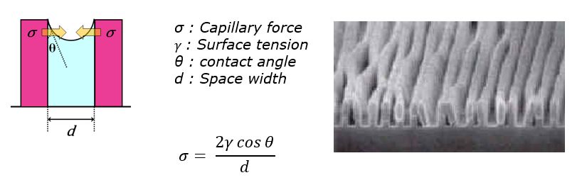 Mitigation Of Pattern Collapse In EUVL Semiconductor Digest
 The Evolving Semiconductor Wafer Size chetanpatil Chetan Arvind Patil
 Imec Ramps Up Development Of High NA EUV Patterning Ecosystem News
 PDF Explorations Of Missing Hole Defect In EUV Patterning
 OptiStack Multilayer Lithography Brewer Science
 Digital Transformation Of The Chemicals Industry Digitalization Of Business Chemical Sector Evolving Semiconductor Characterization And Parametric Test
 Patterning Merck KGaA Darmstadt Germany
 COMPONENT MANUFACTURE LUBRICATION INDUSTRIAL HOME
 December 4 2021 Total Solar Eclipse
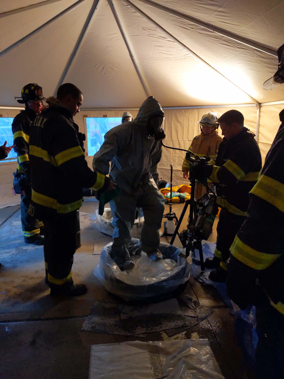 The Evolving Hazmat Front Firehouse
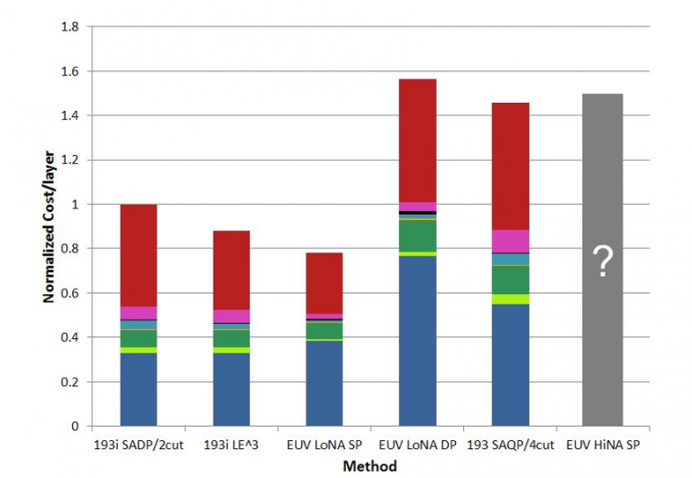 EUV Lithography Extending The Patterning Roadmap To 3nm Semiconductor Digest
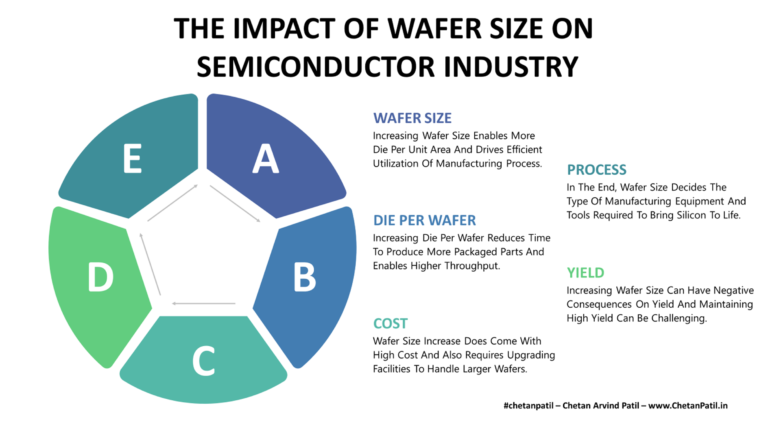 The Evolving Semiconductor Wafer Size chetanpatil Chetan Arvind Patil
 Component Integration The Purchaser s Dream External Feature Smith
 PDF Molecular Glass Resists As High Resolution Patterning Materials Christopher K Ober
  Multi Patterning EUV Vs High NA EUV
 Applied Materials India Sponsors Fellowship Program For CeNSE Students At IISc
 New Clutch Damper Materials Allow For Improved Performance
 The Evolving Semiconductor Wafer Size chetanpatil Chetan Arvind Patil
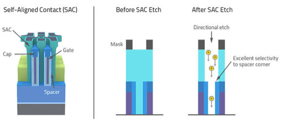 What s Next For Atomic Layer Etch
 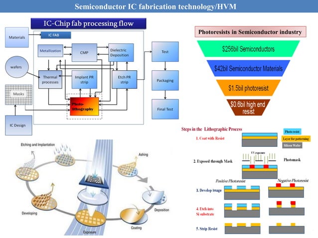 Extreme Ultraviolet Litography EUVL Novel Patterning Materials Progress And Challenges
  Semiconductor Packaging Materials Toppan Printing Co Ltd Electronics Division
 COMPONENT MANUFACTURE LUBRICATION INDUSTRIAL HOME
 Yoshiaki Yoshida All Star 2018
 Worldwide Patterning Materials Industry To 2026Electronic Bharat
 Imec Inpria And TEL Demonstrate Integrated Fab Process For Metal oxide EUV Photoresist
  UHP Panels Cabinets Ultra High Purity Australia
 System Level Test Methodologies Take Center Stage Go Semi And Beyond