EduMission Physics Form 5 Chapter 4 Semiconductor
Free printable calendar template — download, print, and start planning today.
More Like This
 What Is Valence And Conduction Band And Band Gap Of Semiconductor
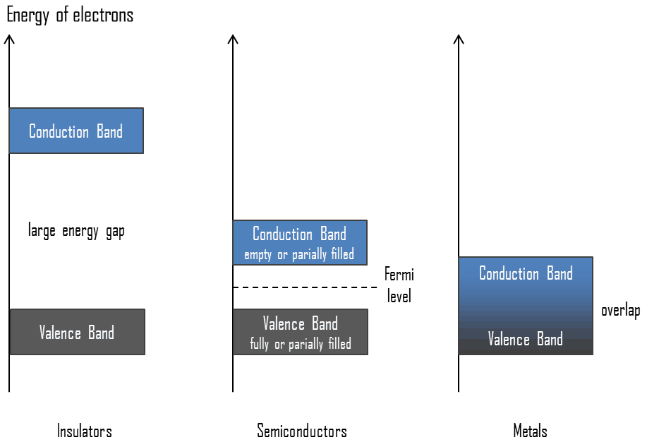 Was Ist Halbleiter B ndermodell Definition
 Energy Bands In Solids Conduction Band And Valence Band By Kushleen
 Difference Between Valence Band And Conduction Band Compare The
 Quantum Mechanics How Can Electrons Travel From The Valence Band Into
 Valence Band Conduction Band And Forbidden Energy Gap By MathOgenius
 What Are Valence Electrons Definition And Periodic Table Chapter 2
 I m With The Valence Band Band Structure And Conduction
 Valence Band Conduction Band And Forbidden Energy Gap YouTube
 NanoHUB Courses Semiconductor Fundamentals Self Paced 2020
  Band Positions top Of Valence Band And Bottom Of Conduction Band Of
 Valence Band Conduction Band Forbidden Energy Gap In Hindi YouTube
 Classification Of Semiconductors Electronics CircuitBread
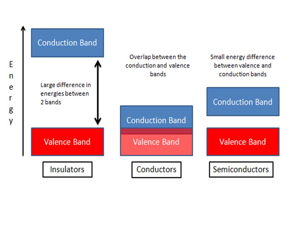
 SEMICONDUCTOR Valence Band Conduction Band Forbidden Energy GapEduMission Physics Form 5 Chapter 4 Semiconductor
 Figure 2 Schematic Representation Of Conduction Band Valence Band
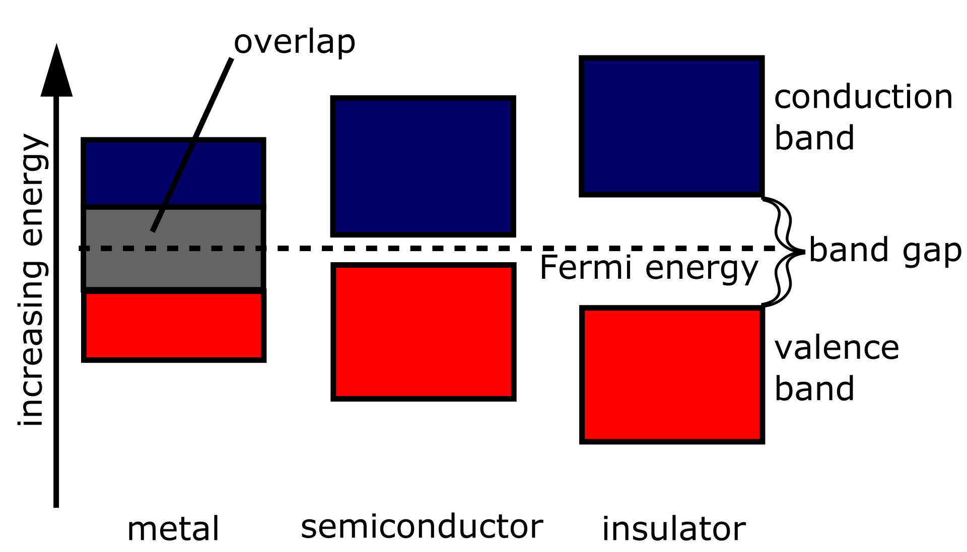 MSE160 Molecules And Materials Engineering Science 2T7 Orientation
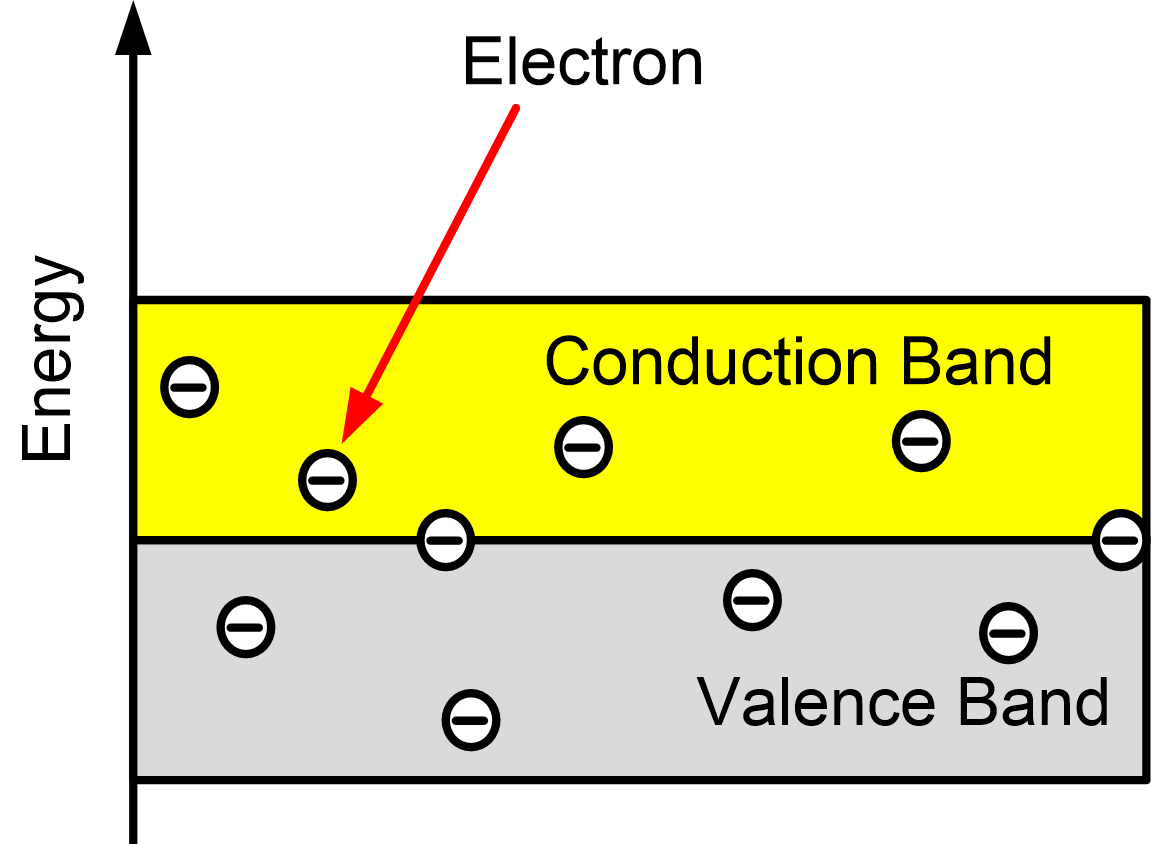 Difference Between Conductor Semiconductor And Insulator Electrical
 Difference Between Valence Band And Conduction Band Compare The
 Valence Band Diagram Difference Between Valence Band And Conduction
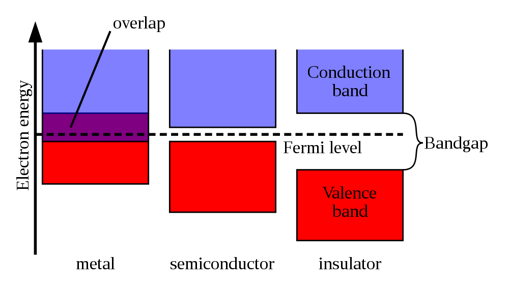 Figure 100 Schematic Showing The Valence And Conduction Bands In A
 Redistribution Of Valence And Conduction Band States Depending On The
 Electronic Band Theory Conduction Of Semiconductors At Atomic Levels
 The Conduction And Valence Bands Of Monolayer WS2 Calculated Using
 A The Conduction Band And Valence Band Diagrams Of Ti Single layer
 Energy Band Diagrams Of Metal And N type Semiconductor Contacts
 Valence Band Conduction Band And Forbidden Energy Gap
 Conduction Band And Valence Band Positions Vs NHE Of Common
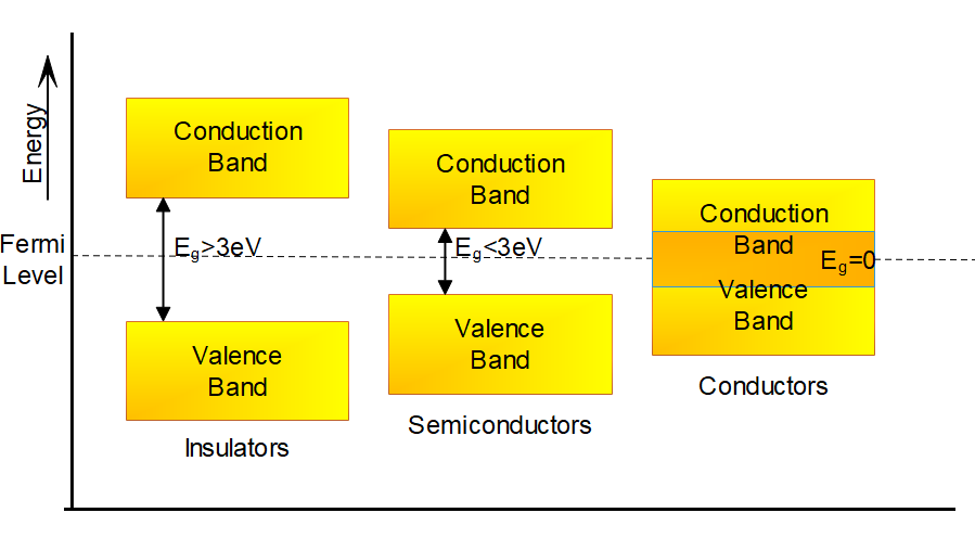 The Distinction Between Conductors Insulators And Semiconductors Is
 If The Band gap Between Valence Band And Conduction Band In A Material
 The Simulated Conduction And Valence Band Diagrams upper Row
 Energy Band Diagrams Of a Conduction Band And b Valence Band Around
 Valence Band And Conduction Band Positions For Ge 20 Te 80 x Sb X x D
 a Variation Of Valence Band Maximum VBM And Conduction Band Minimum
 Valence Band And Conduction Band Definition Energy Bands In Crystals