Electrical Revolution
Free printable calendar template — download, print, and start planning today.
More Like This
 Forbidden Energy Gap In A Semiconductor Is
 Forbidden Energy Gap In A Semiconductor Is YouTube
 Forbidden Energy Gap Of A Semiconductor
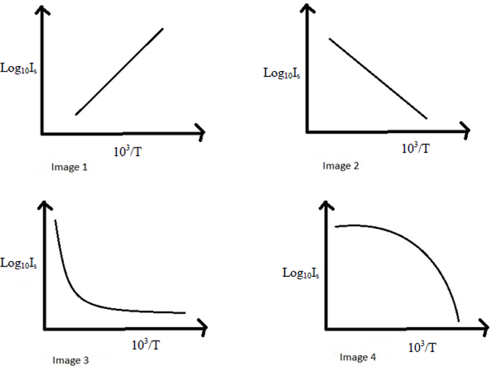 Energy Band Gap Simulation
 In A Semiconductor The Forbidden Energy Gap Between Valence Band And
 Forbidden Energy Gap Of A Semiconductor As The Name Implies This
 The Forbidden Energy Gap In An Intrinsic Semiconductor Is YouTube
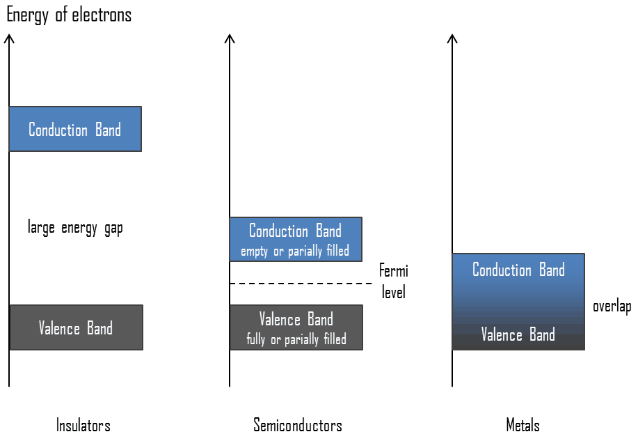 Was Ist Halbleiter B ndermodell Definition
 Forbidden Energy Gap Of Semiconductor Experiment PDF
 Rekvizity Restaurace Br t L ky What Is Band Gap Grafick Astronomie
 B Sc 3rd YearTo Determine The Resistivity And Forbidden Energy Gap Of A
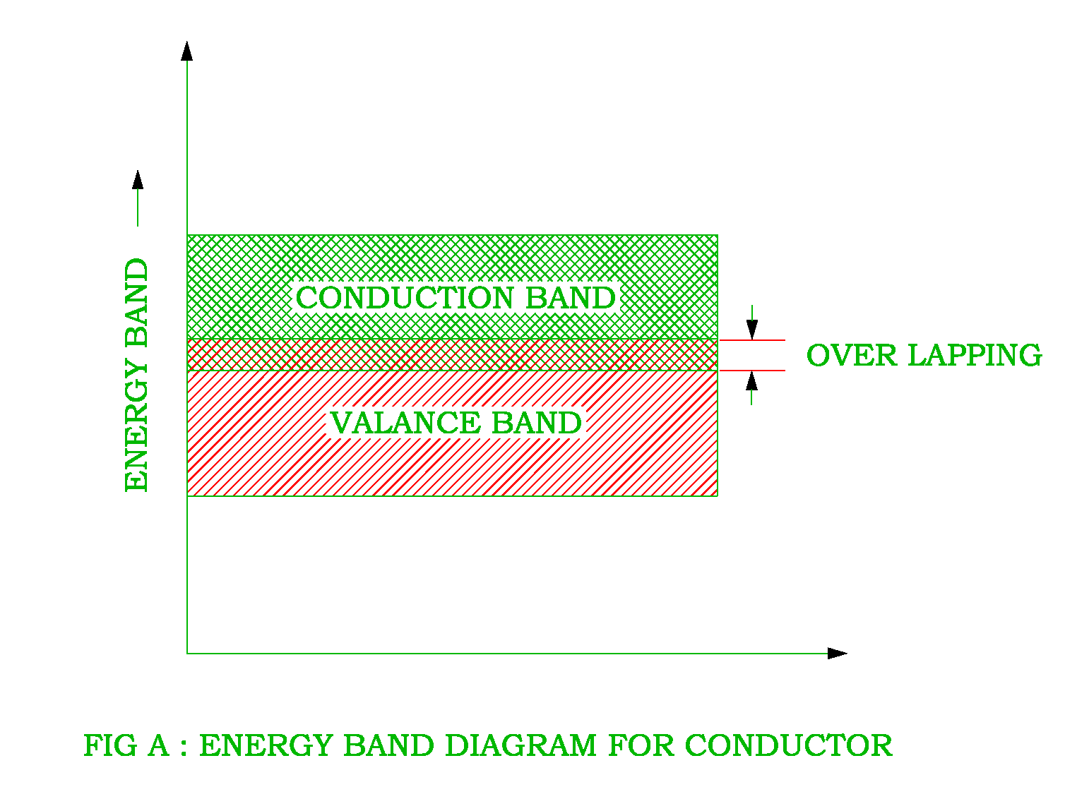
 Electronics 1 SEMICONDUCTOR Valence Band Conduction Band Forbidden
 Forbidden City Beijing China Attractions Lonely Planet
 Valence Band Conduction Band And Forbidden Energy Gap YouTube
 Explain The Difference Between Conductors And Insulators MohamedgroPierce
 To Determine The Energy Band Gap Of The Semiconductor Using A Junction
 What Does Band Gap Mean
  The Forbidden Energy Gap Of Ge Is 0 75 EV The Maximum Wavelength Of
 PDF Experimental Estimation Of The Band Gap In Silicon And Germanium
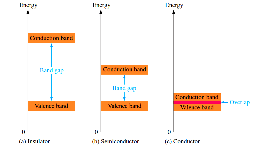 Band Gap For Semiconductor Materials Inst Tools
 The Magnitude Of Forbidden Energy Gap Is
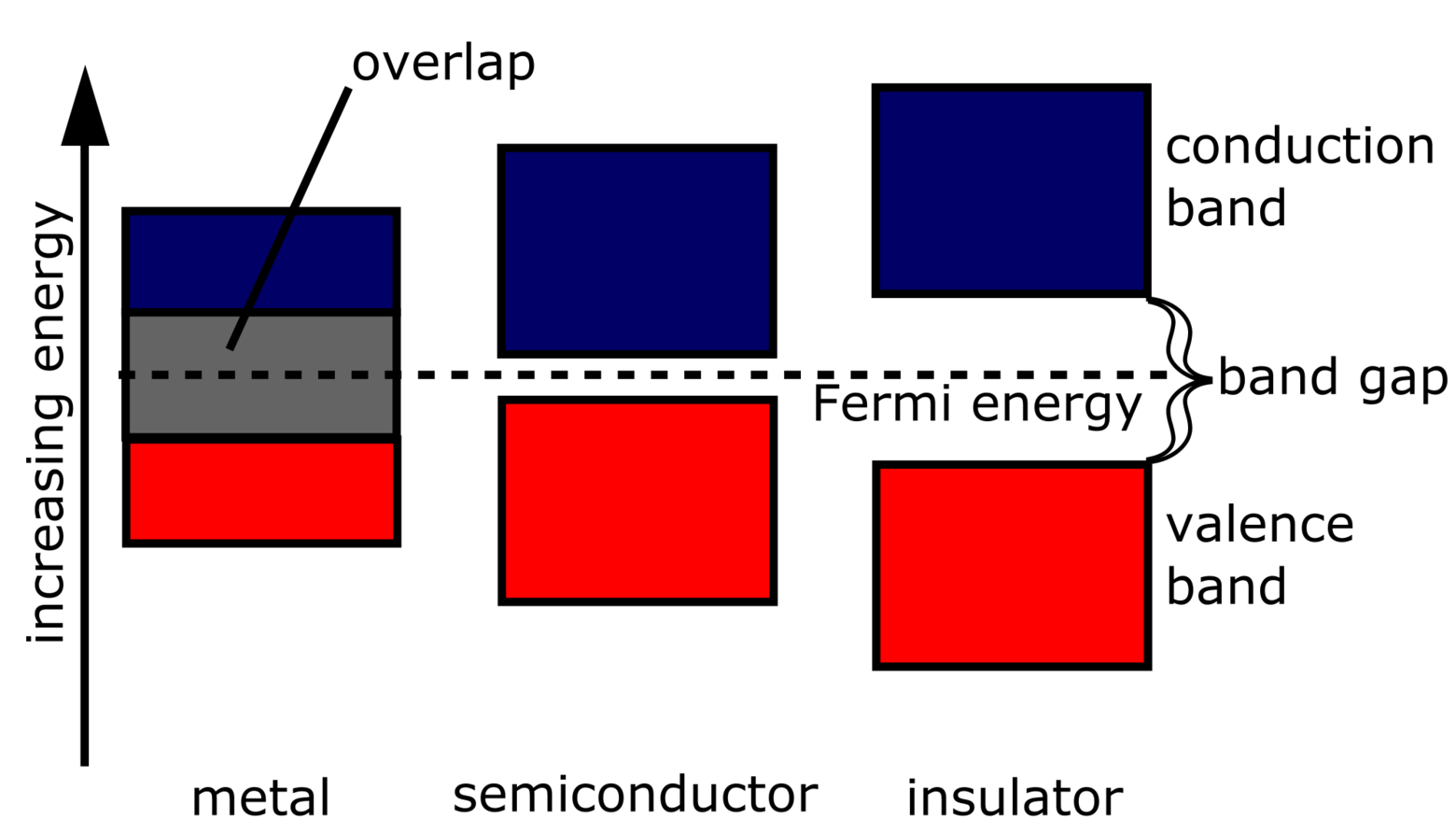 Bande Interdite Maybaygiare
 Kari ra Senio i Nic Uv Vis Band Gap Me ita Ropa Ulo it
 31 Forbidden Energy Gap Of Ge Is 0 75 EV Maximum Wave Length Of
 SEMICONDUCTOR Valence Band Conduction Band Forbidden Energy Gap
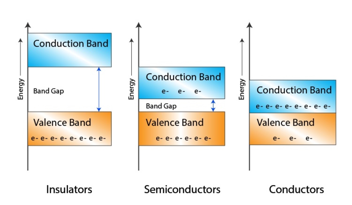 13 Intriguing Facts About Band Theory Facts
 To Determine The Energy Band Gap Of The Semiconductor Using A Junction
 Figure 1 From Experimental Estimation Of The Band Gap In Silicon AndElectrical Revolution
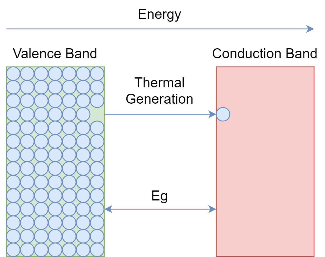 Energy Gap Semiconductor
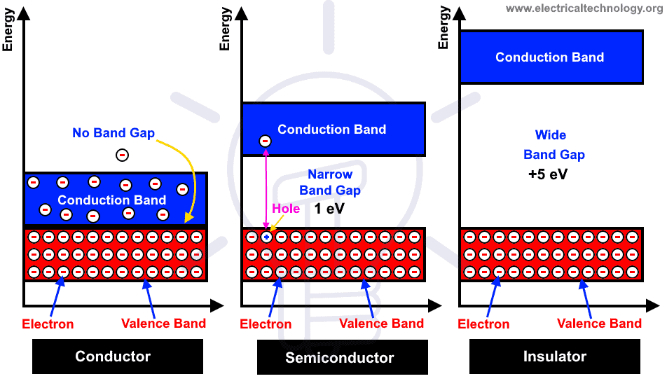 Difference Between Conductor Semiconductor And Insulator
 CLASSIFICATION OF MATERIAL BASED ON BAND GAP
 The Forbidden Energy Gap Of Ge Is 0 75 EV The Maximum Wavelength Of
 Band Gap Energy And Band Gap Edge Positions Of Different Semiconductor
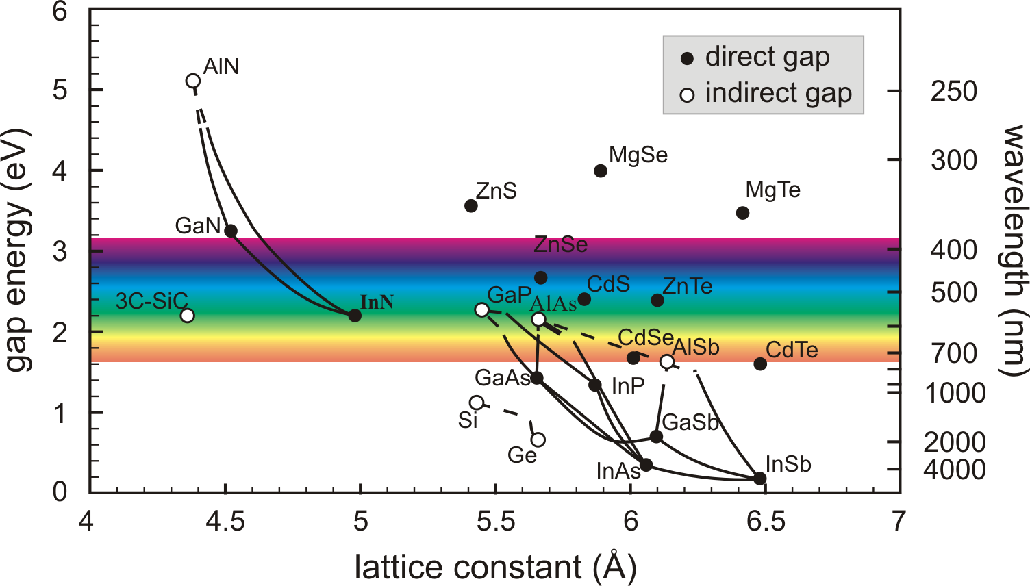 3 III V Compound Semiconductor Material Systems