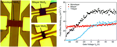
Thickness Dependent Mobility In Two Dimensional MoS2 Transistors
Free printable calendar template — download, print, and start planning today.
More Like This
 a) Device structure of the 2D MoS2 synaptic transistor. b) A schematic ...
 High-performance Gr-contacted MoS2 transistors with STO top-gate ...
 The structure of the MoS2 transistor | Download Scientific Diagram
 (a) Schematic illustration of a top-contact/top-gate MoS 2 transistor ...
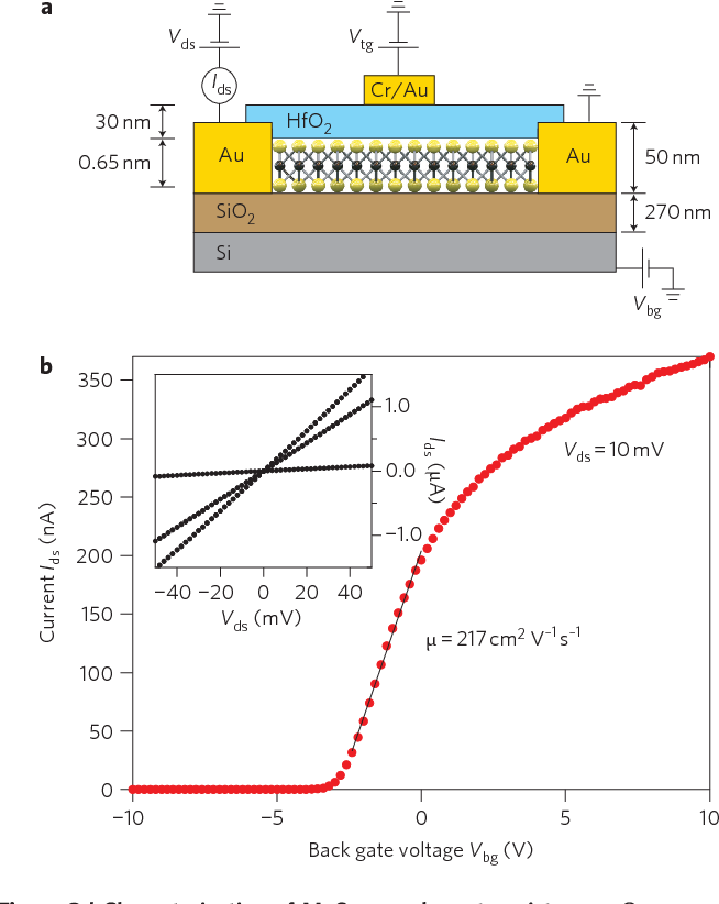 Figure 3 from Single-layer MoS2 transistors. - Semantic Scholar
 Monolayer MoS2 transistors with very high ION a, Transfer... | Download ...
 Flow chart for fabricating a MoS2 transistor biosensor: (a) printing of ...
 Atomic sectional drawing (a) of a MoS2 transistor with graphene ...
 2D MoS2 Filament transistor (FFET). a) Schematic diagram. Adapted with ...
 (PDF) Multiple MoS2 Transistors for Sensing Molecule Interaction Kinetics
 Breakdown of High-Performance Monolayer MoS2 Transistors | ACS Nano
 (a) Schematic of MoS2 transistor with Au NPs decoration, (b) scanning ...
 (a) Schematic illustration of the MoS2 transistor-based NO2 gas-sensor ...
 2D MoS2 Filament transistor (FFET). a) Schematic diagram. Adapted with ...
 Structure of stacked MoS2 transistors with optimized contact structure ...
 Energy diagrams for the MoS2 neuron transistor. (a) Schematic view of ...
 Breakdown of High-Performance Monolayer MoS2 Transistors | ACS Nano
 Electrical performance of TMDCs field-effect transistors. (a,c,d ...
 a) 3D schematic illustration of a four‐electrode MoS2 transistor. b ...
 MoS2 transistors ‒ LANES ‐ EPFL
 (a) Schematic illustration of the MoS2 transistor-based NO2 gas-sensor ...
 Mos2 Field-Effect Transistor For Next-Generation Label-Free Biosensors ...
 Performance characterization of the MoS2 transistors a, Isd–Vg curves ...
 SEM images of the fabricated top-gated MoS2 transistors: (a) transistor ...
 MoS2 inverter. a) Schematic diagram of a MoS2 inverter. MoS2 PFET was ...
 Two-Terminal MoS2 Memristor and the Homogeneous Integration with a MoS2 ...
 (a) Schematic image of the monolayer MoS2 based transistor. (b) Optical ...
 Transfer characteristics of MoS2 transistors with deposited and ...
 Electrical characteristics of MoS2 transistors, TLM and contact‐end ...
 (a) Schematic layout of our double-gated MoS2 FETs. The top gate ...
 Integrated Circuits Based on Bilayer MoS2 Transistors | Nano Letters
 (a) MoS2 transistor with Au source and drain contacts. Only n-type ...
 (a) A MoS2 thin film transistor and its transport properties. (b) Drain ...
 (a) Transfer characteristics of the BP/MoS2 vdWH transistor at Vds = +1 ...
 Electrical properties of MoS2 TFTs a Schematic image of MoS2 TFTs. b ...
 (a) Key process steps of the fabrication of the monolayer MoS2 ...
 MoS2 RF Transistor Suki Zhang 02/15/ ppt download
 a) 3D schematic illustration of a four‐electrode MoS2 transistor. b ...
 A Photoelectric-Stimulated MoS2 Transistor for Neuromorphic Engineering ...
 a) 3D schematic illustration of a four‐electrode MoS2 transistor. b ...
 (a) Transfer curves of dual-gated MoS2 transistor when V tg sweeps from ...
 Process for fabricating the dual-gate MoS2 field-effect transistors ...
 P‐Type Polar Transition of Chemically Doped Multilayer MoS2 Transistor ...
 Figure 2 from Improved Interfacial and Electrical Properties of MoS2 ...
 Schematic illustration of a biased monolayer MoS2 transistor. The ...
 Two-Terminal MoS2 Memristor and the Homogeneous Integration with a MoS2 ...
 Electrical characterization of the few-layer MoS2 transistor. (a,b) are ...
 a) Schematic illustration of MoS2 transistor‐array‐based... | Download ...
 Journal of Semiconductors
 High-density vertical sidewall MoS2 transistors through T-shape ...
 High performance of edge-contacted PtTe2-MoS2 metal-semiconductor ...
 MoS2 transistors with 1-nanometer gate lengths | Science
 a) 3D representation of the structure of MoS2. b) Schematic ...
 Output characteristics of the Pre-15 MoS2 transistor for (a) all ...
 (PDF) Self-screened high performance multi-layer MoS2 transistor formed ...
 Two-Terminal MoS2 Memristor and the Homogeneous Integration with a MoS2 ...
 Simulation of MoS 2 stacked nanosheet field effect transistor
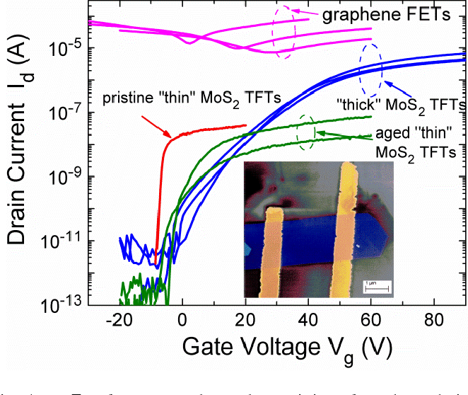 Figure 1 from 1/ $f$ Noise Characteristics of MoS2 Thin-Film ...
 a) Optical image of a back‐gate monolayer MoS2 transistor; the scale ...
 The fabrication procedure of MoS2 transistors: (a) the MoS2 as-grown ...
 I–V characteristics MoS2 transistors with various contact structures a ...
 Output characteristics of the MoS2 transistor without annealing ...
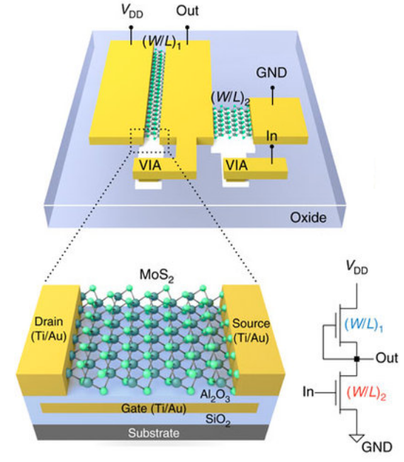 The first 2D microprocessor — based on a layer of just 3 atoms | Kurzweil
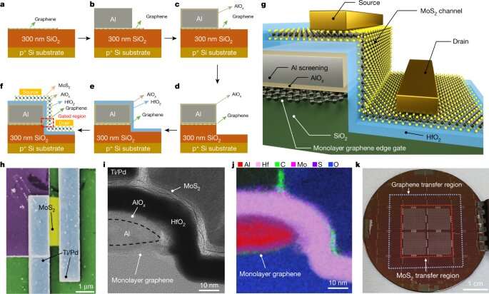 Creating sub-1-nm gate lengths for MoS2 transistors
 MoS2 transistors with 1-nanometer gate lengths | Science
 | MoS 2 transistor performance. a, Fabrication process of MoS 2 ...
 MoS2 monolayers make GHz transistor – National Nanotechnology Center ...
 High Performance Multilayer MoS2 Transistors with Scandium Contacts ...
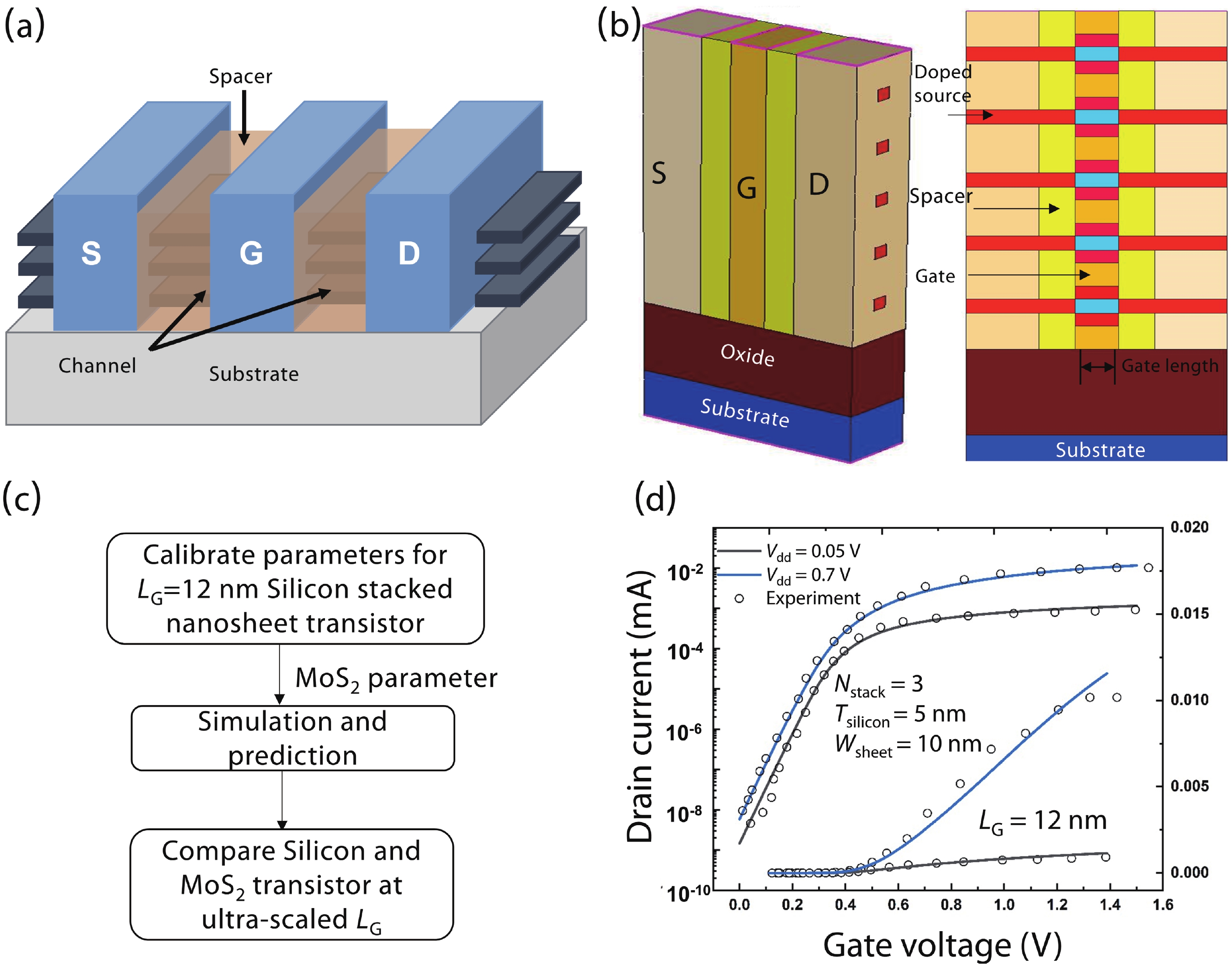 Simulation of MoS 2 stacked nanosheet field effect transistor
 (a) Schematic layout of our double-gated MoS 2 FETs. The top gate ...
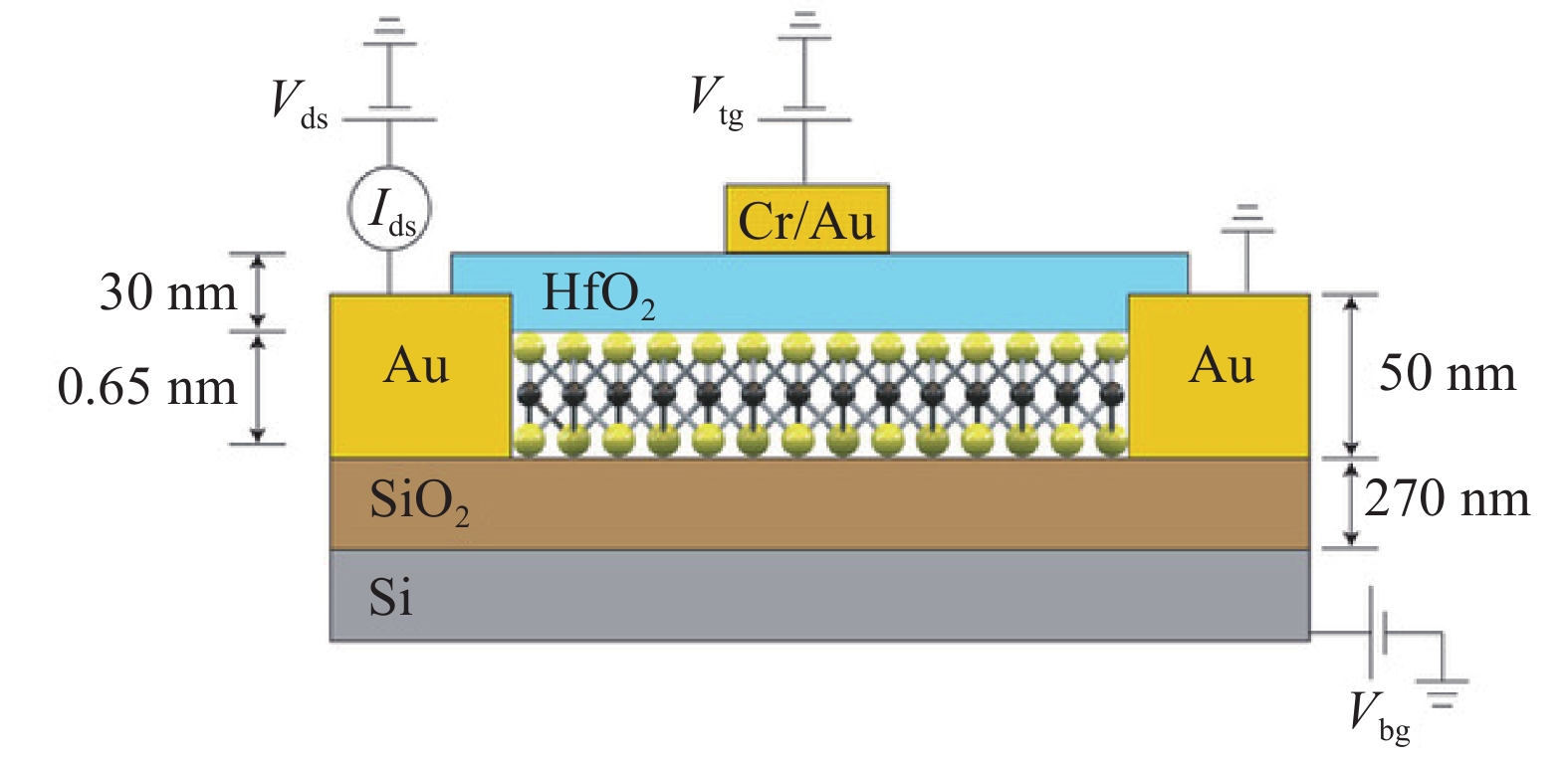 Research progress and challenges of two dimensional MoS 2 field effect ...
 Two-Terminal MoS2 Memristor And The Homogeneous Integration, 57% OFF
 (a) Optical image of prepared MoS2 transistor on the Al2O3/ITO/SiO2/Si ...
 Inkjet-Printed MoS2 Transistors with Predominantly Intraflake Transport ...
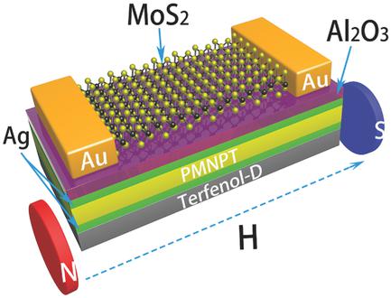 Magnetic‐Induced‐Piezopotential Gated MoS2 Field‐Effect Transistor at ...
 Tuning Schottky Barrier of Single-Layer MoS2 Field-Effect Transistors ...
 Quasi-1-Dimensional Dual-Gate MoS2 Field-Effect Transistors with 50 nm ...
 Edge-Contact MoS2 Transistors Fabricated Using Thermal Scanning Probe ...
 Side‐Gate BN‐MoS2 Transistor for Reconfigurable Multifunctional ...Thickness-dependent mobility in two-dimensional MoS2 transistors ...
 A scalable approach for MoS 2-field-effect transistors with low contact ...
 Ambient effects on electrical characteristics of CVD-grown monolayer ...
 Metal Semiconductor Field-Effect Transistor with MoS2/Conducting NiOx ...
 Electrical effects of 4ATP on MoS2 transistor. a) Device structure ...
 Micromachines | Free Full-Text | Hysteresis in As-Synthesized MoS2 ...
 Output and transfer characteristics of MoS2-channel transistors with ...
 a) Schematic illustration of MoS2 transistor‐array‐based... | Download ...
 13.High-density vertical sidewall MoS2 transistors through T-shape ...
 (a) Fabricated MoS2 transistor devices on polyimide (PI) substrates ...
 a) Schematic of a MoS2 memtransistor device. b) ID–VD curves with ...
 Figure 6 from High-performance MoS2 transistors with low-resistance ...
 Flow chart for fabricating a MoS2 transistor biosensor: (a) printing of ...
 Energies | Free Full-Text | MoS2 Transistors with Low Schottky Barrier ...
 a) Schematic illustration of MoS2 transistor‐array‐based... | Download ...
 Plug-and-probe devices on 2D materials a, Transfer curves of the MoS2 ...
 (a) MoS2 transistor with Au source and drain contacts. Only n-type ...
 Performance characterization of the MoS2 transistors. (a) Transfer ...
 Self-screened high performance multi-layer MoS2 transistor formed by ...
 A Photoelectric-Stimulated MoS2 Transistor for Neuromorphic Engineering ...
 (a) Inkjet printable MoS2 ink and its flexible photodetector. (b ...
 Breakdown of High-Performance Monolayer MoS2 Transistors | ACS Nano
 Back-gated planar MoS2 transistors (a) The measured structure. The ...