
Multiple Patterning Semiconductor Engineering
Free printable calendar template — download, print, and start planning today.
More Like This
 What Is Patterning Education Destination Malaysia
 Nikon AF S NIKKOR 24 70 Mm F 2 8E ED VR Mieten Ab 8 86 Am Tag
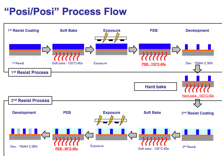 A Simple Approach To Litho Litho Etch Processing Utilizing Novel
 DANIELA Fl gelt rschrank 4 Fachb den 5 Ordnerh hen Gaerner Deutschland
 Was Ist SkyShowtime Und Wo Ist Es Erh ltlich
 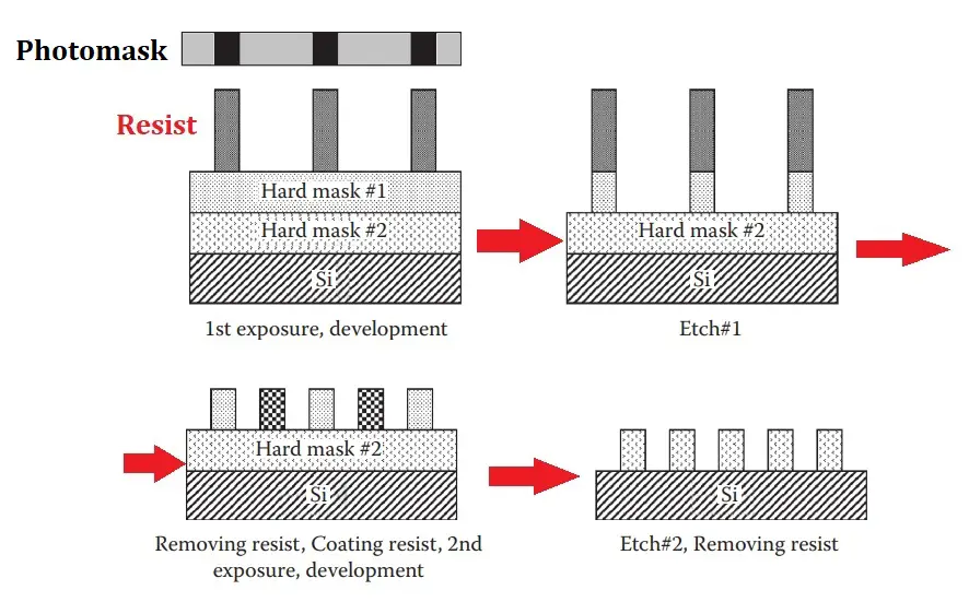 Double Patterning Siliconvlsi
 Der Papst Kommt Nach Irland Das Wird Kein Heimspiel Irland News
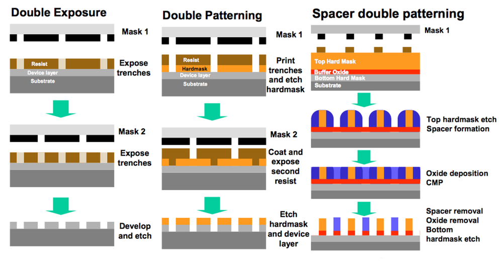 Sadp Tutorial Youtube
 Paulo Coelho Quotes Be Yourself Zitate F r Das Leben
 Schematic Sketches Of The Wet etching SAM Fabrication Process 1
 berdachung Grundeinheit Gaerner Deutschland
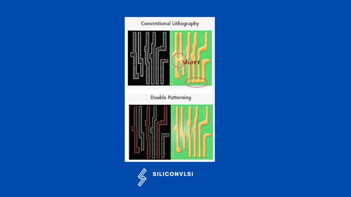 Why We Used Double Patterning In VLSI Siliconvlsi
 Angebot Aldi S d Belavi Solar Gartenleuchte Mit
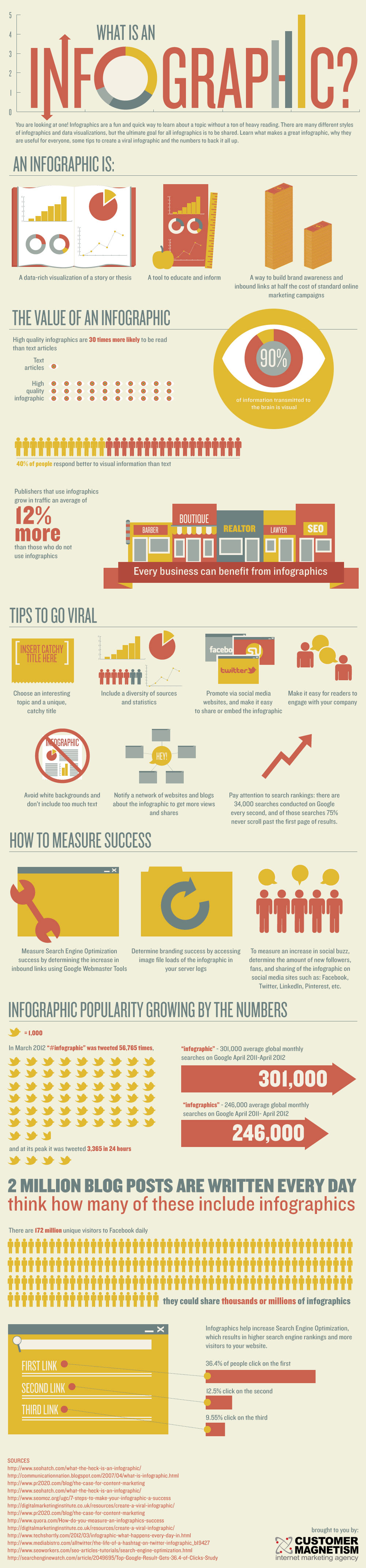 Webinar LPM Saarbr cken Making The Most Of Infographics Nik Peachey
 Patterning Solutions Merck KGaA Darmstadt Germany
 Solcellepanelteknologi Hjelper Stanford forskere Med Lage OLED
 File 360 Wave Process Hair Waves jpg Wikimedia Commons
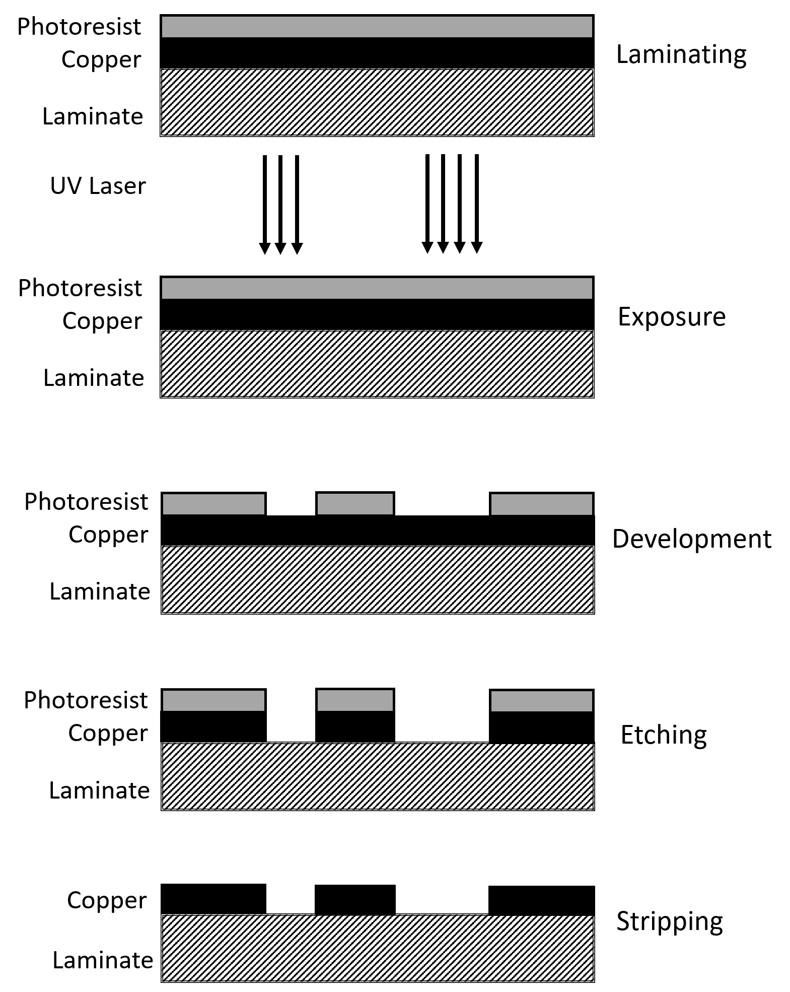 Laser Direct Imaging And Its Advantages Sierra Circuits
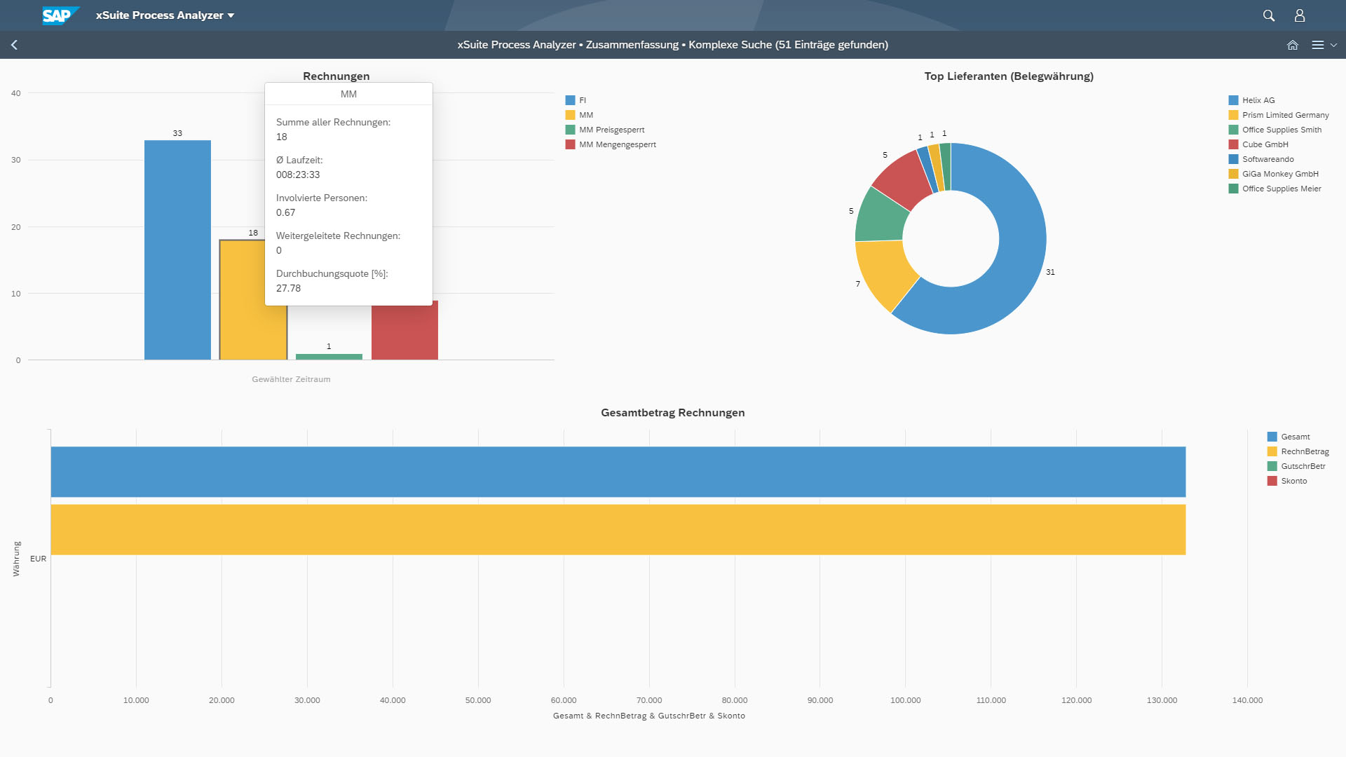 Invoice XSuite
 CD SEM Images At 6 Steps In The Contact Patterning Process Download
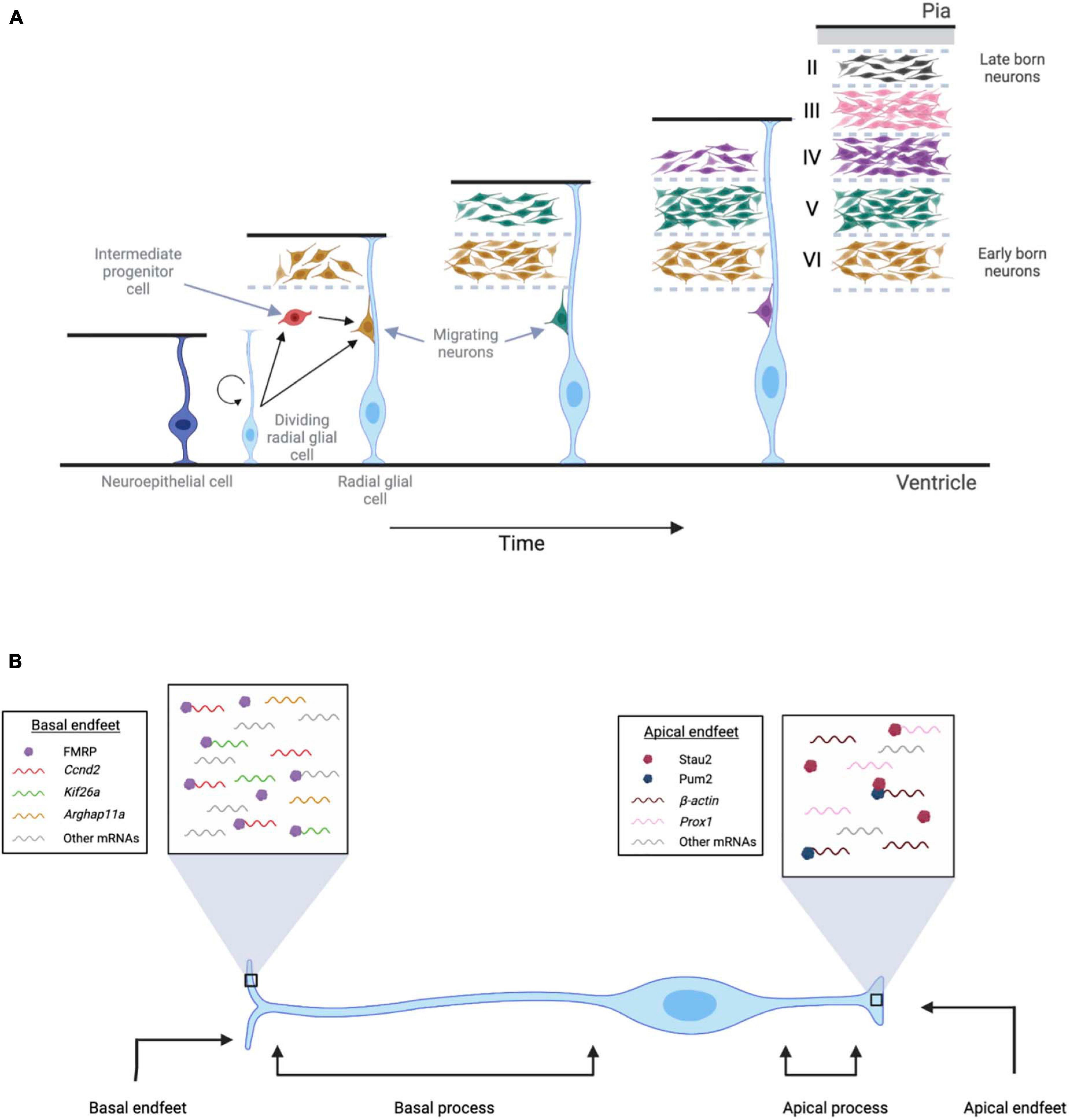 Frontiers Local Translation Across Neural Development A Focus On
 Table I From Design patterning Co optimization Of SRAM Robustness For
 Multi patterning Strategies For Navigating The Sub 5 Nm Frontier Part
 Introducing Patterns To Toddlers Preschoolers Busy Toddler
 VLSI Symposia Samsung Use EUV For 7 Nm Process Elektor Magazine
 Kostenlose Foto Pfad Stra e Rasen Spiel Junge Kind Denken Gr nMultiple Patterning Semiconductor Engineering
 Double Patterning Lithography Double The Trouble Or Double The Fun
  Kostenlose Foto Blatt Bl tenblatt Rot Botanik Flora Rote Blume
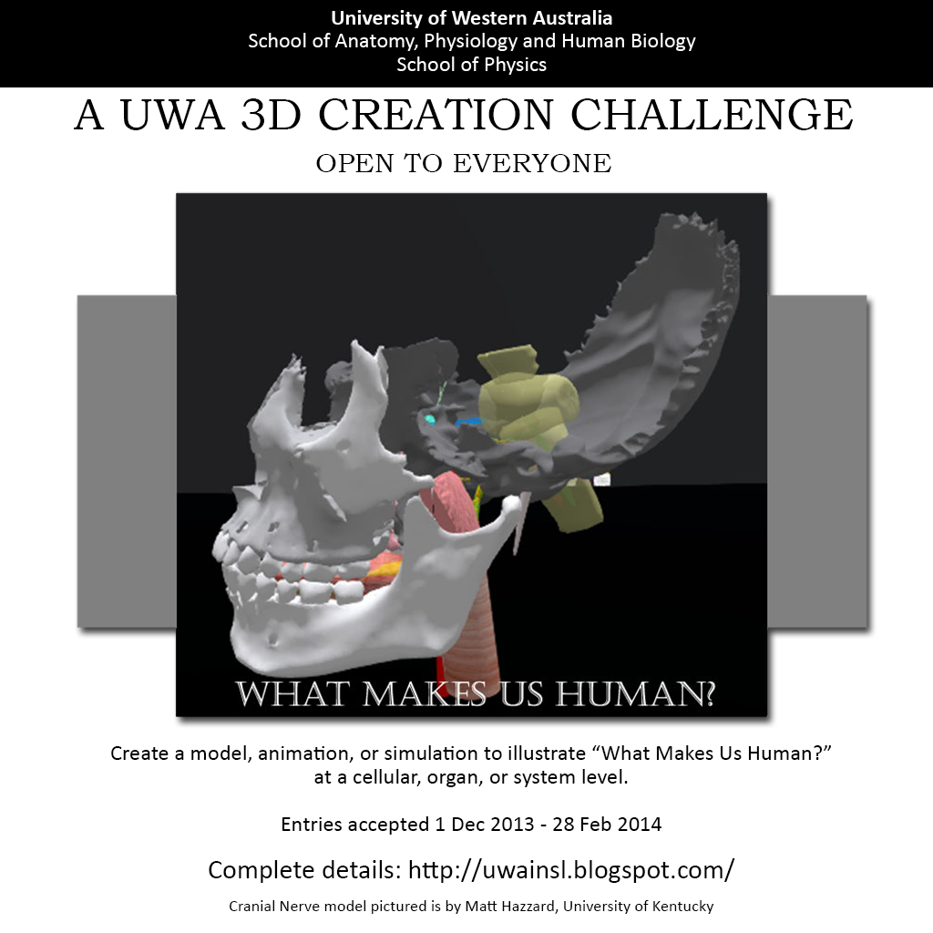 Echt Virtuell UWA 3D Bauwettbewerb Was Macht Uns Zum Menschen
 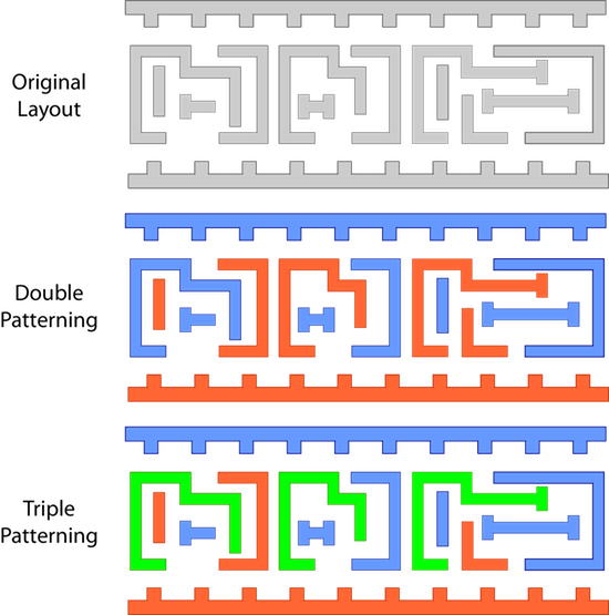 Uniting Lithography Sign off Simulation And Multi patterning From 20nm
 Why Is Patterning So Important To Your Child s STEM Fluency STEM
 Semiconductor Manufacturing Southland Sensing Ltd