Vlsi
Browse our collection of Vlsi templates. Each calendar is free to download and optimized for printing on standard paper sizes. Click any image to view the full-size version and download it instantly.
 Figure 1 VLSI Design Verification And Test Flow
 Power Grid Analysis In VLSI Designs | Semantic Scholar
 Imbedded Vs Embedded What s The Difference The Word Counter
 The Need For Static Timing Analysis In VLSI Design Flow YouTube
 PhysicalDesignForYou VLSI Physical Design Flow
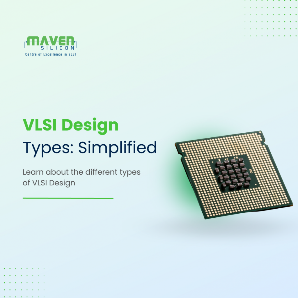 Types Of Vlsi Design Tool Design Talk
 Antenna effect in VLSI Fabrication | Plasma Induced Gate Oxide Damage | Plasma Etching - YouTube
 VLSI Design - Useful Resources
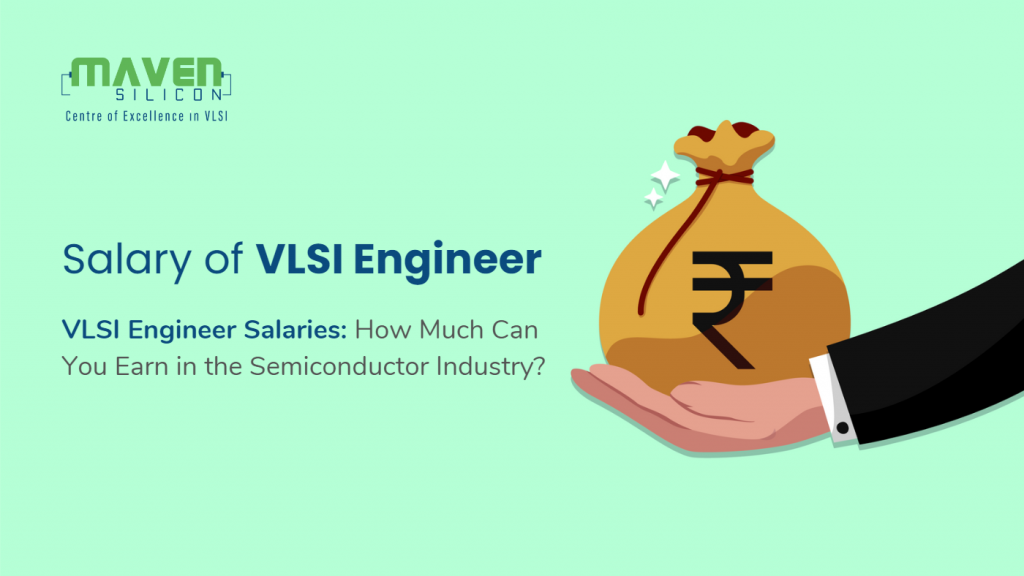 Salary Of VLSI Engineers In India Maven Silicon
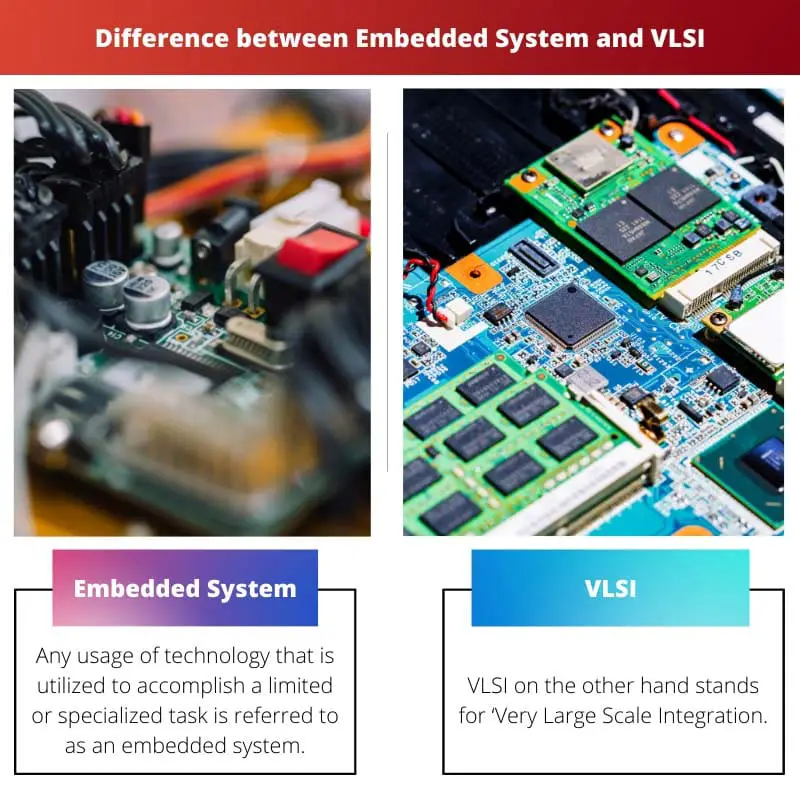 Difference Between Embedded System And VLSI
 Cmos Vlsi Design A Circuits And Systems Perspective United States
  Traditional design flow (with emphasis on power grid | Download Scientific Diagram
 VLSI Design Engineer Job Description Velvet Jobs
 GitHub RadhaKulkarni26 Y Chart in VLSI In This Repositroy I Have Explained Y Chart Used In
  LeadSOC Technologies VLSI Embedded Software Design
 What Is VLSI Very Large Scale Integration An Overview
 What to Learn to Enter into the VLSI Industry ? Learning for VLSI | QnA | EP-6 - YouTube
 VLSI Physical Design 33 Hours Of Video AvaxHome
 Implementation Of A Static Timing Analyser VLSI
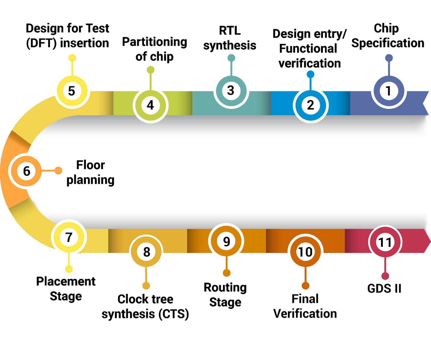 ASIC
ASIC  Benefits Of A VLSI Internship
 Antenna Effect Siliconvlsi
 What Is Antenna Effect In VLSI TechSimplifiedTV in
 What Is Synthesis In VLSILeadSOC Technologies VLSI Embedded Software Design
 What Are The Types Of VLSI Design Maven Silicon
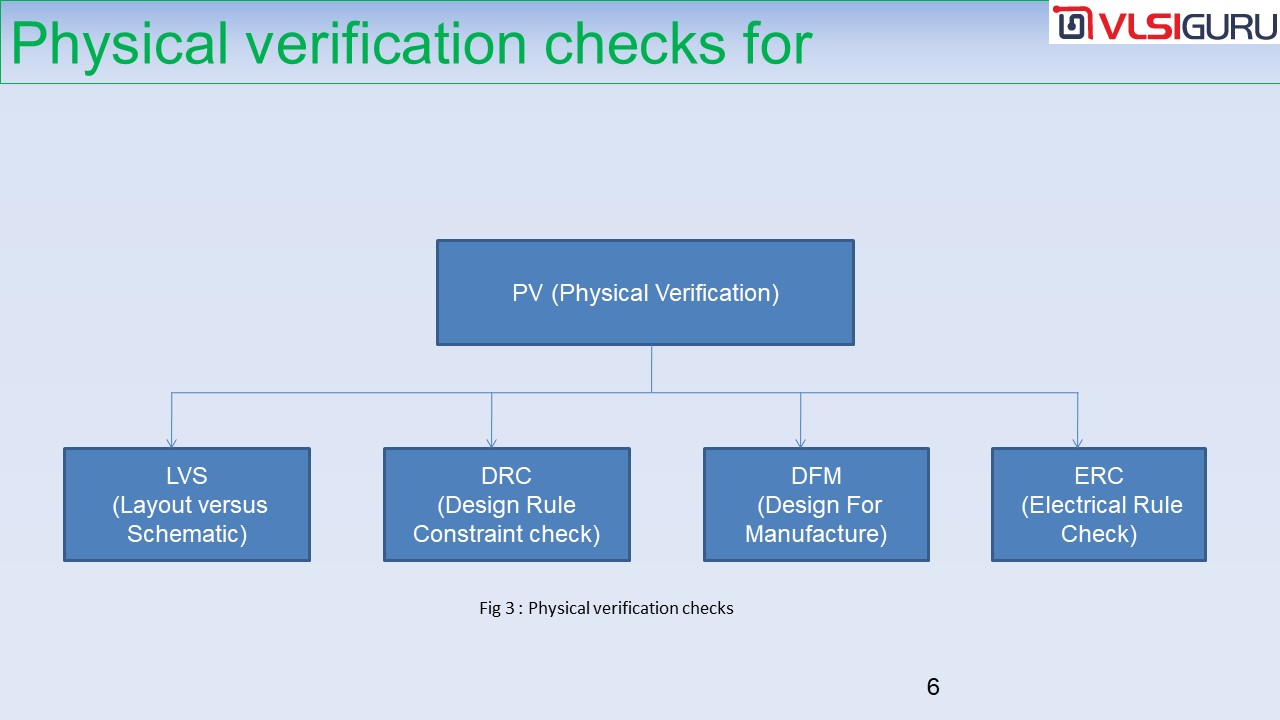 Physical verification slides VLSI Guru
 2011 CMOS VLSI Design A Circuits And Systems Perspective 4th Edition
 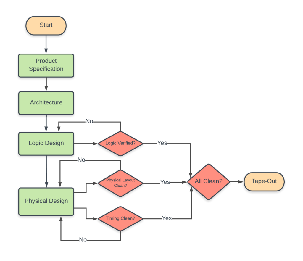 ASIC Design Flow – The Ultimate Guide - AnySiliconThe Need For Static Timing Analysis In VLSI Design Flow YouTube
 What Is Vlsi Design What Are The 5 Levels In VLSI Design What Is VLSI Very Large Scale Integration An Overview
 ASIC Design Flow In VLSI Engineering Services A Quick Guide 2022
  VLSI Design And Verification Monkfox
![ASIC Design Flow for VLSI Engineering Teams [GUIDE] - Xinyx Design](https://www.xinyxdesign.com/wp-content/uploads/2022/08/Frame-2-3.jpg) ASIC Design Flow for VLSI Engineering Teams [GUIDE] - Xinyx DesignWhat Is VLSI Very Large Scale Integration An OverviewWhat Is VLSI Very Large Scale Integration An Overview
ASIC Design Flow for VLSI Engineering Teams [GUIDE] - Xinyx DesignWhat Is VLSI Very Large Scale Integration An OverviewWhat Is VLSI Very Large Scale Integration An Overview Emulation In VLSI Functional Verification Simulation FormalWhat Is VLSI Very Large Scale Integration An Overview
 Standard cell VLSI design: A tutorial | Semantic Scholar
 ⨘ } VLSI } 8 } Antenna Effects } LE PROF } - YouTube
 Standard cell VLSI design: A tutorial | Semantic Scholar
 VLSI Salary In India How Much Extra A VLSI Engineer Can Earn CTC
 Static Timing Analysis STA YouTube
 VLSI Circuit And System Design Engineering Sciences
 Antenna Effects | Physical Verification | Back To Basics - YouTube
 VLSI Design Engineer Job Description Velvet Jobs
 Synthesis Signoffsemiconductors
 PPT Algorithms For VLSI Design Automation PowerPoint Presentation
 Dynamic Timing Analysis In VLSI Constraints Modeling And Verification
 Final Year Project For ECE Arduino Sign Language Glove A Complete
 What Is Static Timing Analysis In VLSI
  1 VLSI Physical Design Flow Download Scientific Diagram
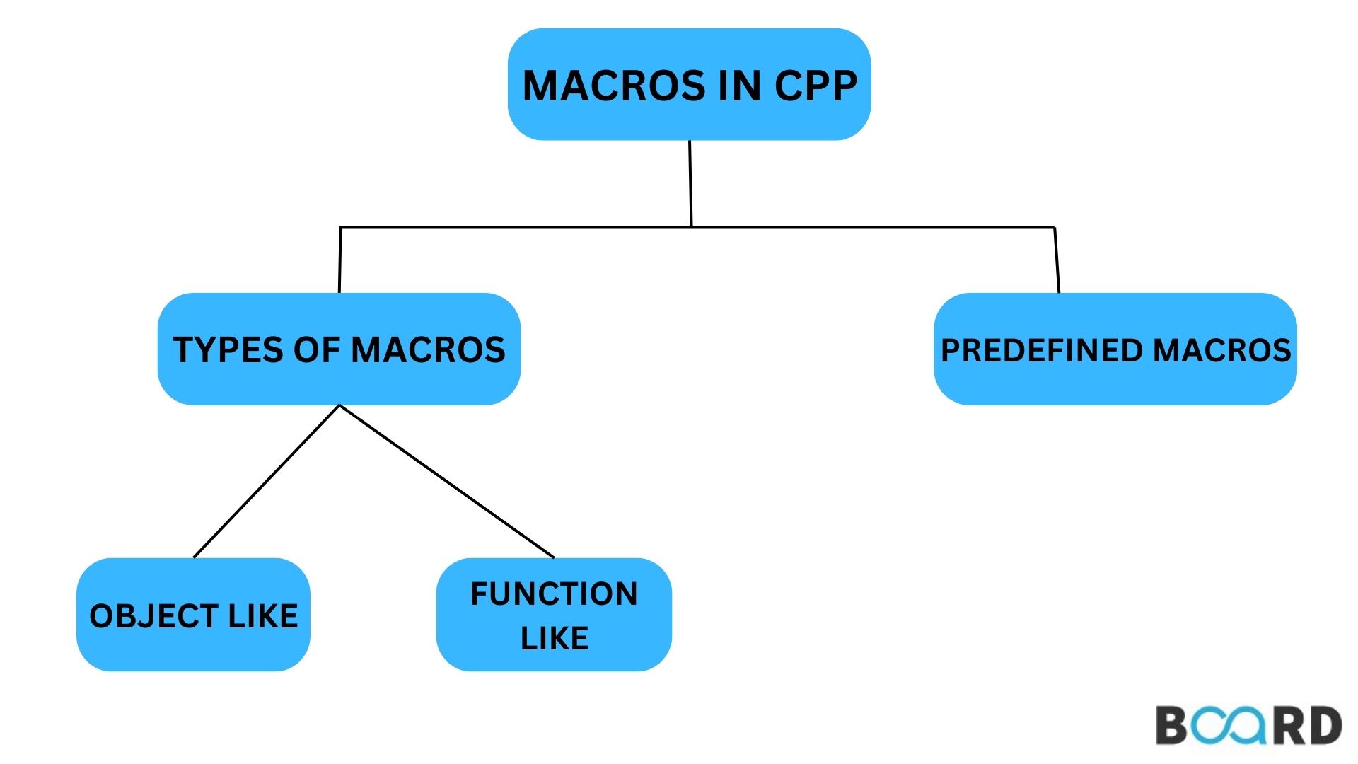 Macros In C Board Infinity
 Mantra VLSI Physical Design Interview2
 Types Of Delay In VLSI
 ASIC Design Flow in VLSI Engineering Services – A Quick Guide
 ECE Final Year Project Major Project For ECE StudentsWhat Is VLSI Very Large Scale Integration An Overview
 VLSI Design Services FPGA Design Services VLSI Engineering
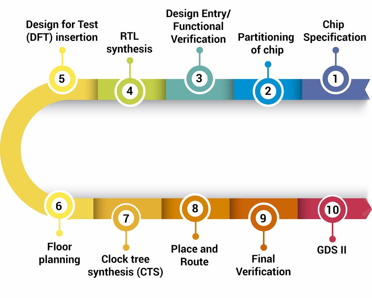 ASIC Design Flow in VLSI Engineering Services — A Quick Guide | by eInfochips ( An Arrow Company) | eInfochips | MediumStatic Timing Analysis STA YouTube
 VLSI Design Module 2 Part 5 Inverter Delays Rise Time Fall Time
  VLSI Physical Design Powerplan YouTube
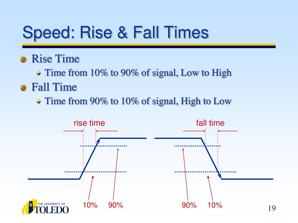 PPT Logic Families PowerPoint Presentation Free Download ID 3964088
 VLSI Design Syllabus EC6601 Regulation 2013 Anna University Free
 Types Of VLSI Design Flows Download Scientific Diagram
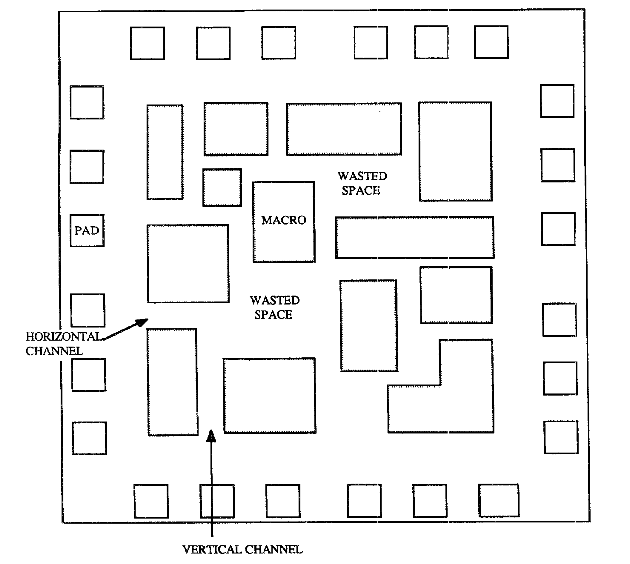 VLSI Cell Placement Technique Enfow s Blog
 Cmos Vlsi Design 3rd Edition Pdf Gamingintensive
 Computing Pioneer To Receive Honorary U M Doctorate
 VLSI Design Rules 3 YouTube
 Difference Between Embedded And Mobile Technology Nadan Academy
 Types Of Delay In VLSI
 Types Of Delay In VLSI
 VLSI Design Flow VLSIFacts
 VLSI Career Who Gets A Higher Salary GitHub RadhaKulkarni26 Y Chart in VLSI In This Repositroy I Have
  What Is Antenna Effect In VLSI TechSimplifiedTV in
 VLSI Talent And Issues India Specific Overview Defence Research And
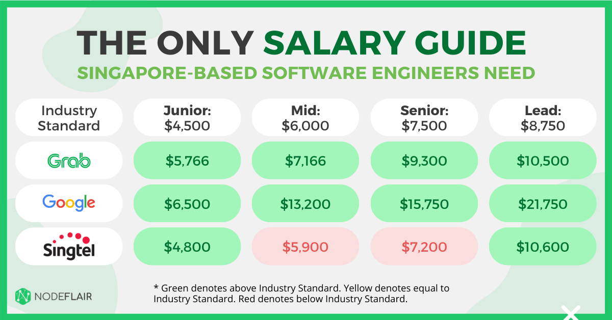 The Only Salary Guide Singapore Based Software Engineers Need
 VLSI QnA: Digital Design Interview Questions - v1.2What Is VLSI Very Large Scale Integration An Overview
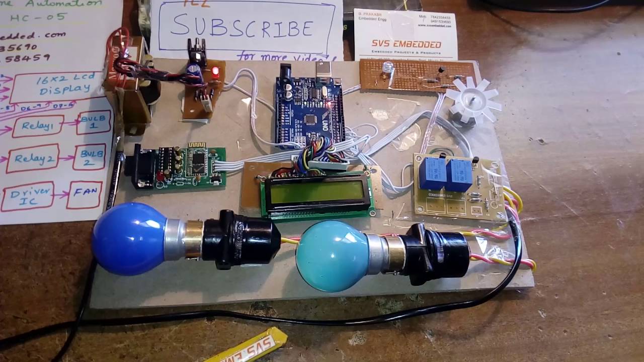 SVSEMBEDDED 9491535690 7842358459 Best Electronics Final Year
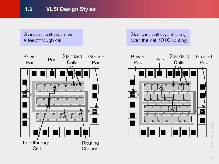 KLMH VLSI Physical Design From Graph Partitioning
 VLSI Design Engineer Job Description Velvet Jobs
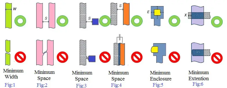 Layout Design Rule Stick Diagrams Siliconvlsi Analog DesignSalary Of VLSI Engineers In India Maven Silicon
 Vlsi Design Flow Chart With Explanation Design Talk
 Power Grid Analysis In VLSI Designs | Semantic ScholarLeadSOC Technologies VLSI Embedded Software Design
 What Is VLSI Design Flow Step By Step Guide
 VLSI Career In US After BTECH Or MTECH Salary Reallocation
  VLSI Full Form Very Large Scale Integration JavaTpoint
 Download PDF CMOS VLSI Design A Circuits And Systems Perspective
 What Is Physical Design In Vlsi Design Talk
 Layout Design RulesVLSI Full Form Very Large Scale Integration JavaTpoint
Layout Design RulesVLSI Full Form Very Large Scale Integration JavaTpoint VLSI
VLSI Antenna Effect Prevention Techniques in VLSI Design - YouTubeVLSI Physical Design: Powerplan - YouTube
 VLSI Beginner Laptop Desktop Configuration ? QnA ! - YouTube
 VLSI DESIGN AND EMBEDDED SYSTEMS Technical Seminar 2015VLSI Design And Verification Monkfox
 VLSI Physical Design Engineer Job Opportunities In Electronics PartVLSI Physical Design Powerplan YouTube
 ECE Final Year Project Major Project For ECE StudentsDifferent Types Of Design Rules In Vlsi Design Talk
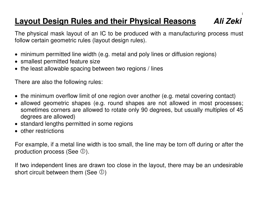 PDF Layout Design Rules And Their Physical Reasons
 Buy VLSI Circuit Design Methodology Demystified A Conceptual Taxonomy PhysicalDesignForYou VLSI Physical Design Flow
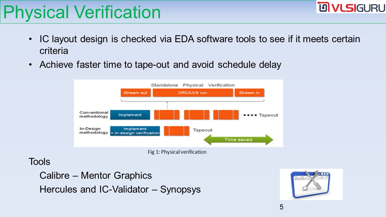 Physical verification slides VLSI Guru
 Difference : Simulation Vs Emulation in VLSI ? QnA ! - YouTube
 PPT EE466 VLSI Design Lecture 6 Logical Effort PowerPoint
  VLSI Design L8 Layout Design Rules YouTube
 PPA Trade offs For Dynamic Timing Analysis In VLSI
 VLSI Design Engineer Job Description Velvet Jobs PDF Layout Design Rules And Their Physical Reasons
 Physical Design In VLSI VLSI POINT