Packaging Process Flow
Browse our collection of Packaging Process Flow templates. Each calendar is free to download and optimized for printing on standard paper sizes. Click any image to view the full-size version and download it instantly.
 2013 SUSS MicroTec Technology Forum Focuses On 3D TSV Infrastructure
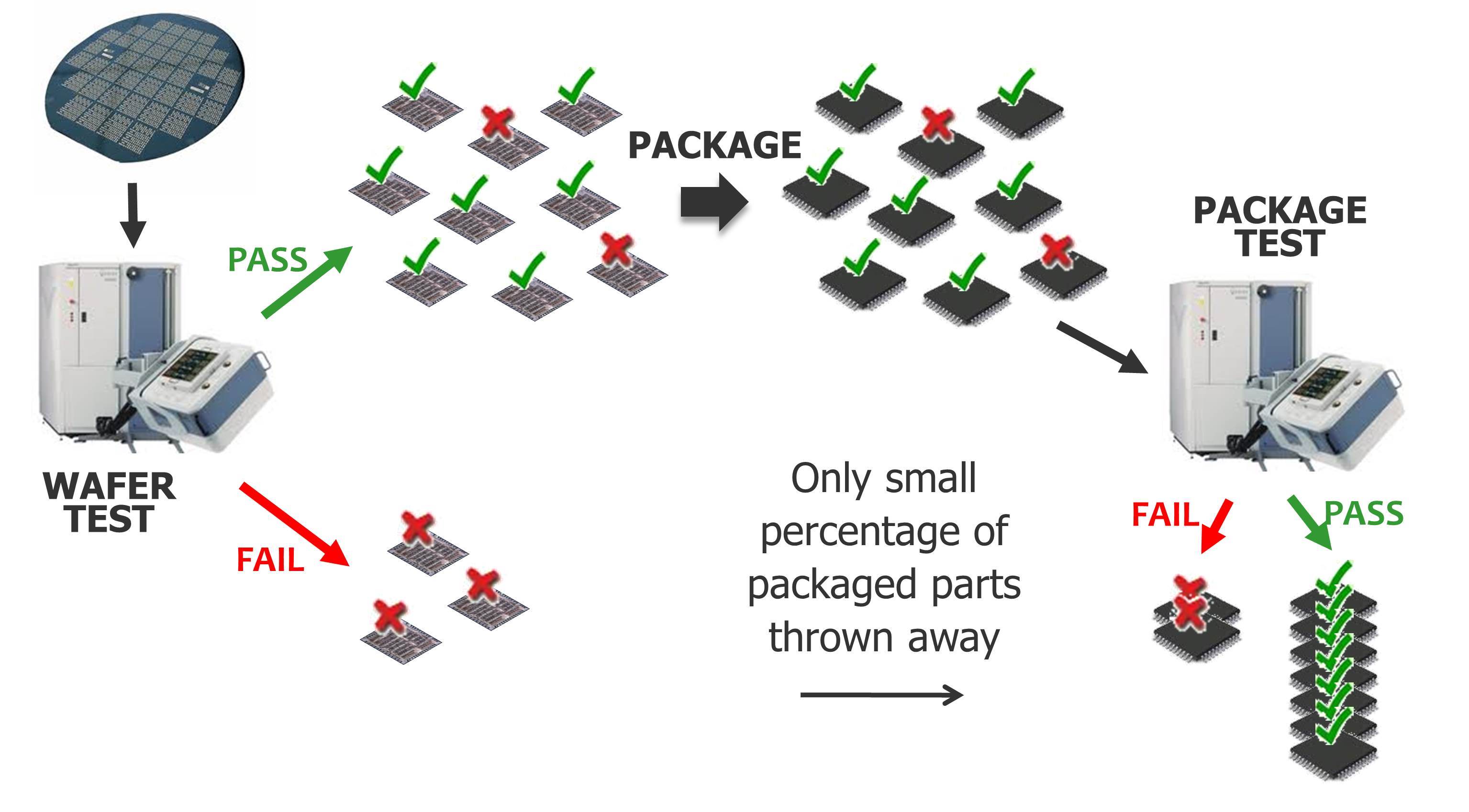 3D IC Test Now And The Road Ahead Tessent Solutions
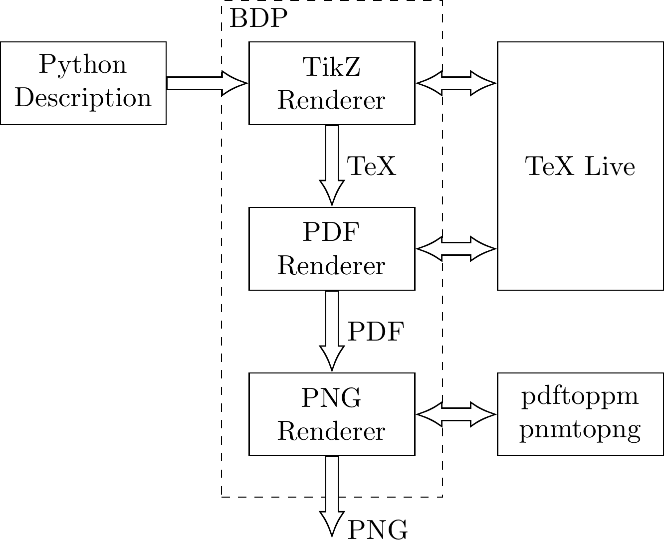 Welcome To BDP Bdp 0 1 Documentation
 Electroplating IC Packages
 IC Packages Why The Variety Rush PCB
 Complete Packaging Solutions Our Process
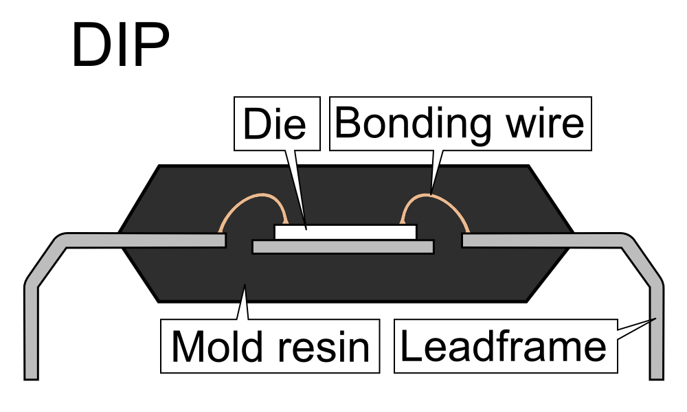 Learning To Decapsulate Integrated Circuits Using Acid Deposition
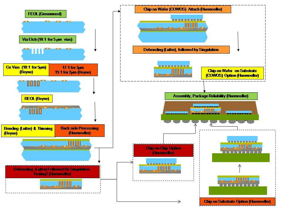
 Conventional Process Flow For 2 5D 3D IC Integration chip On
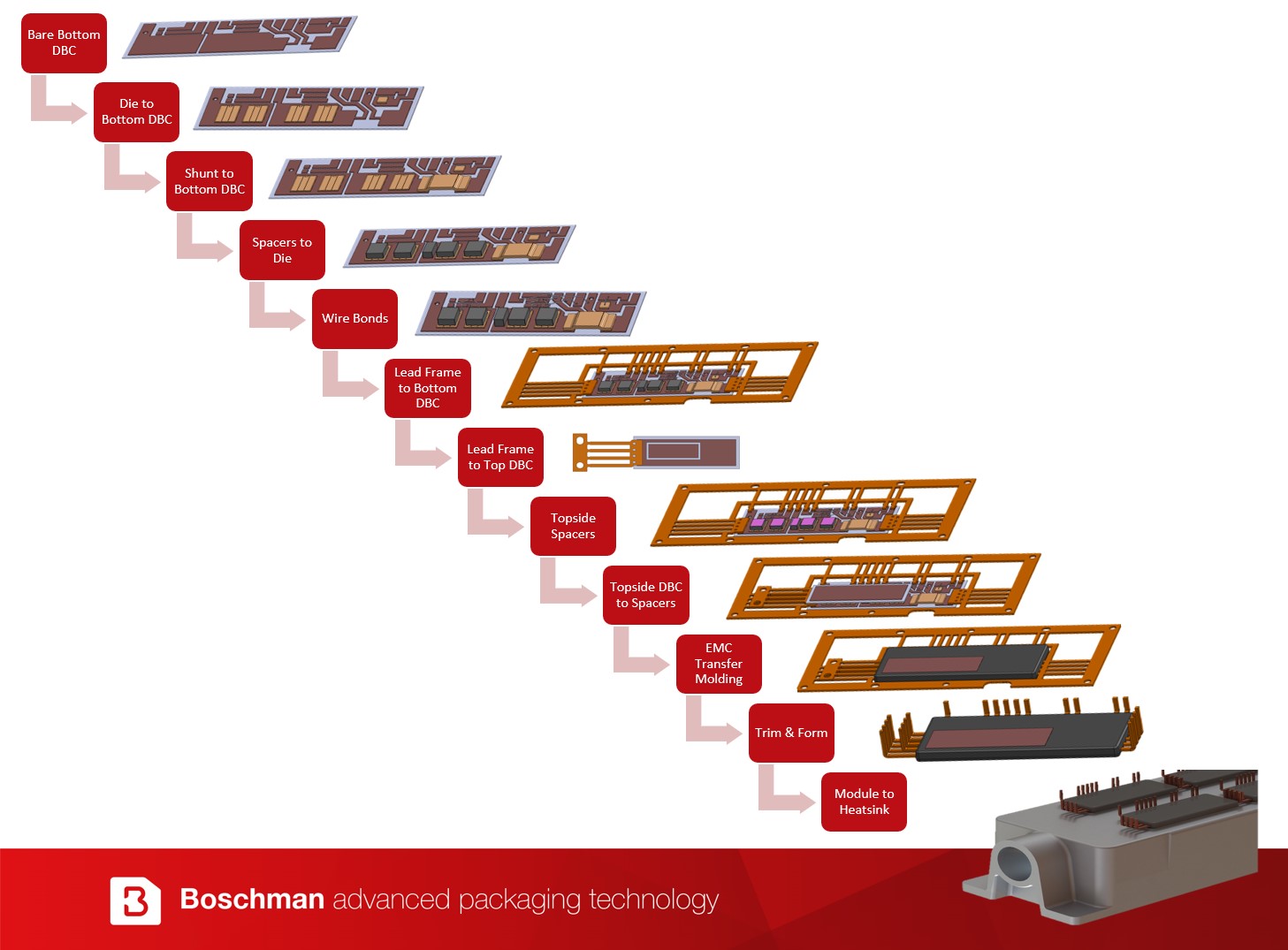 Package Development For Power Modules NDC International
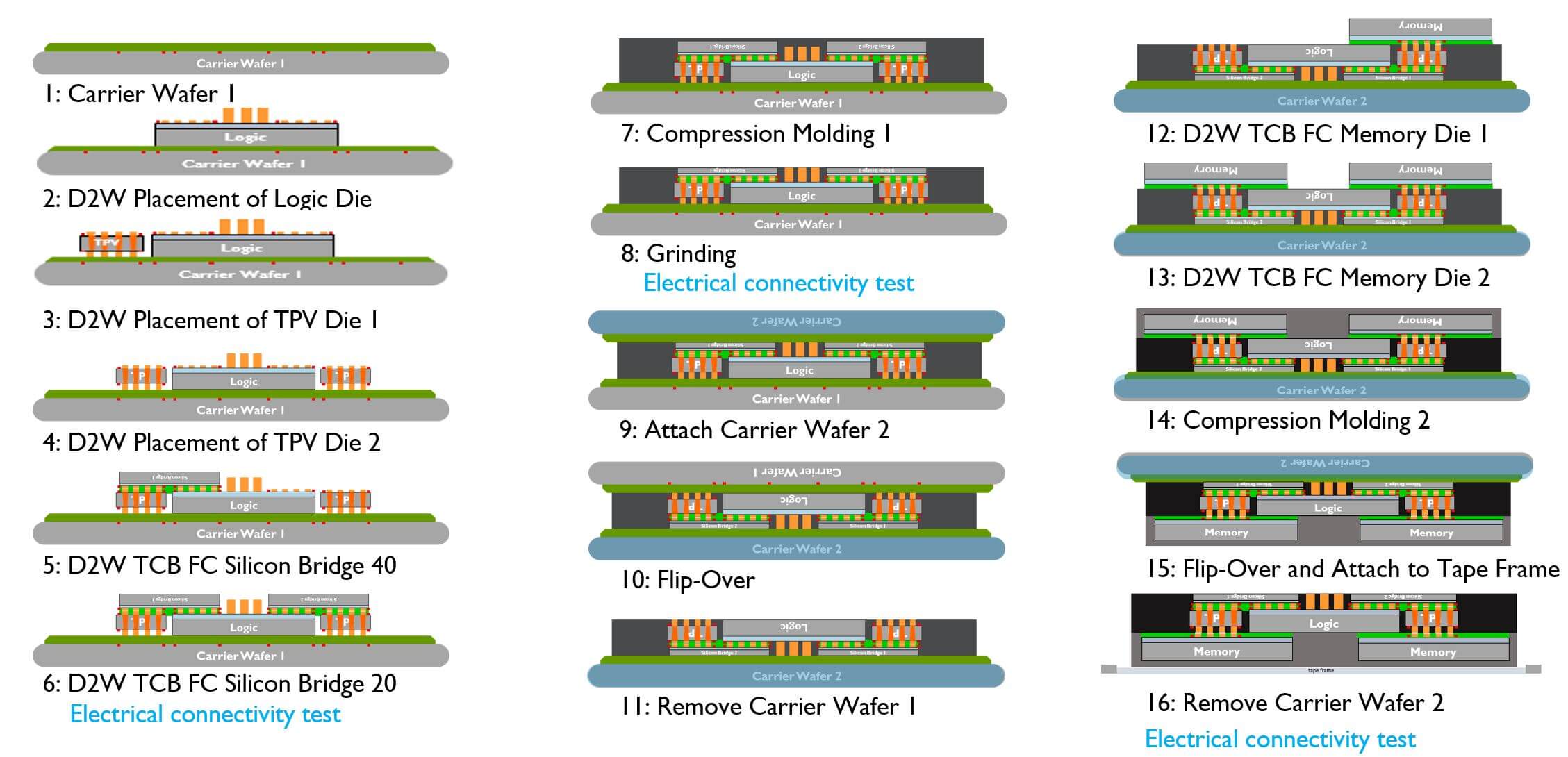 Imec Figure 2 Process Flow 3D InCites
 Semiconductor Packaging ASSEMBLY PROCESS FLOW YouTube
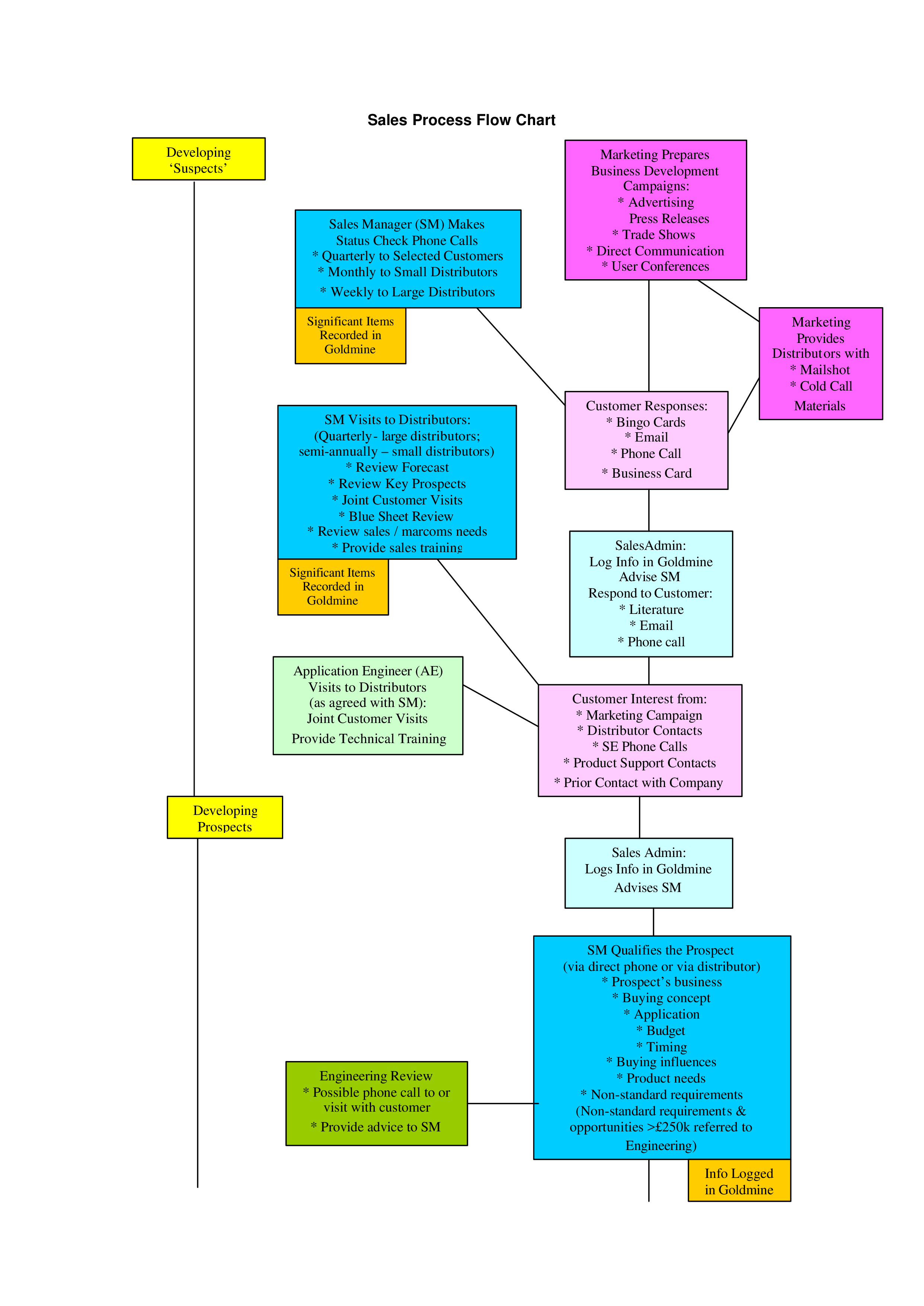 Sales And Marketing Process Flow Chart Templates At
 Packaging Process Flow
 Process Flow Of The Low Temperature Co fired Ceramic LTCC Package
 Fabrication Process
 Order And Delivery Processing In 2021 Process Flow Chart Process
 EDA On Board With New Package Options
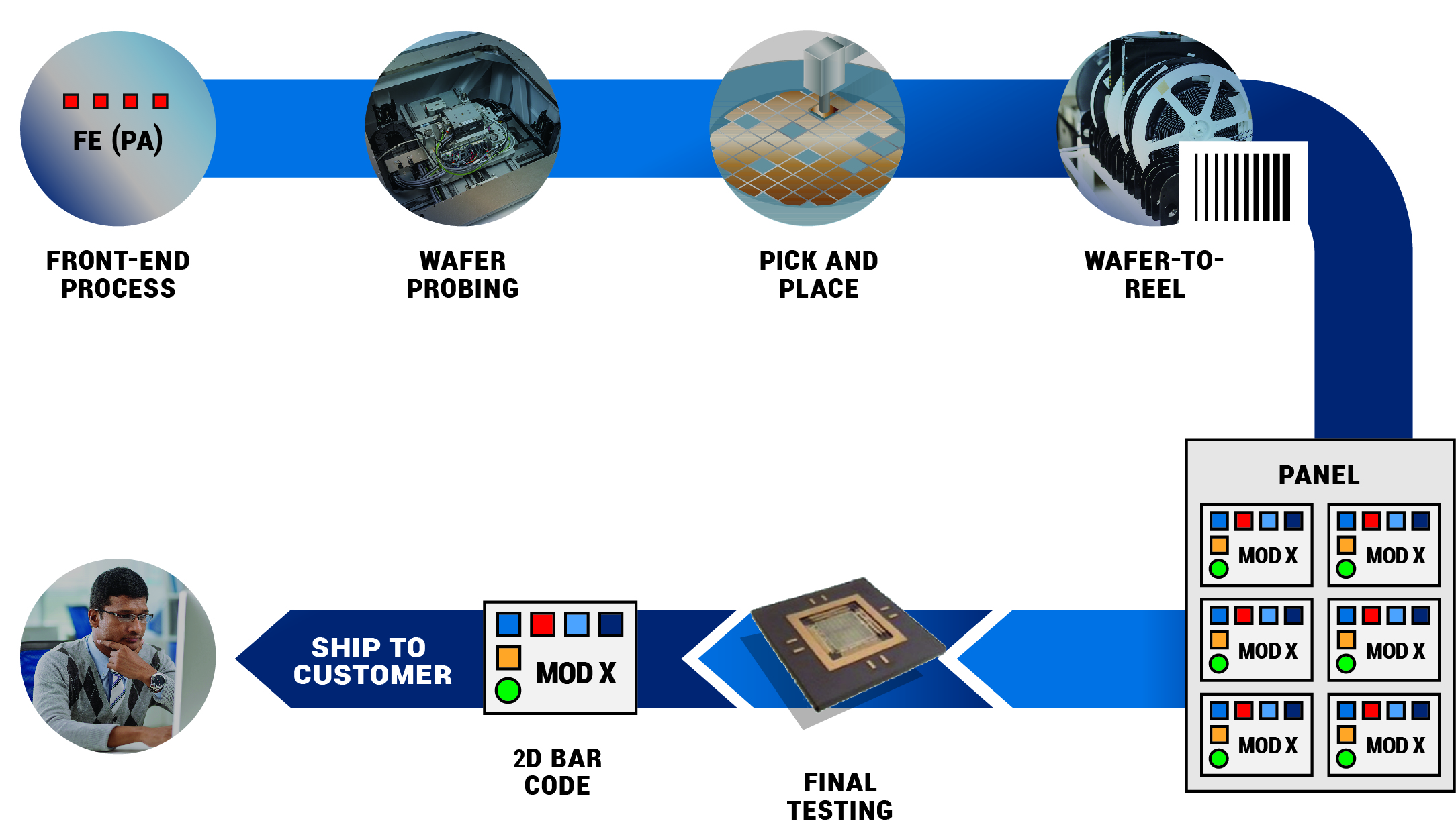 Wafer Fabrication Process Flow Chart
 Biden Precisa De Mais De US 52 Bilh es Para Conter A China Em Chips
 Semiconductor Manufacturing Front end Process sites RIKEN KEIKI Co Ltd
  High Bandwidth Memory White Paper AnySilicon
 Figure 2 From Void Formation Study Of Flip Chip In Package Using No
 Finding Defects In IC Packages
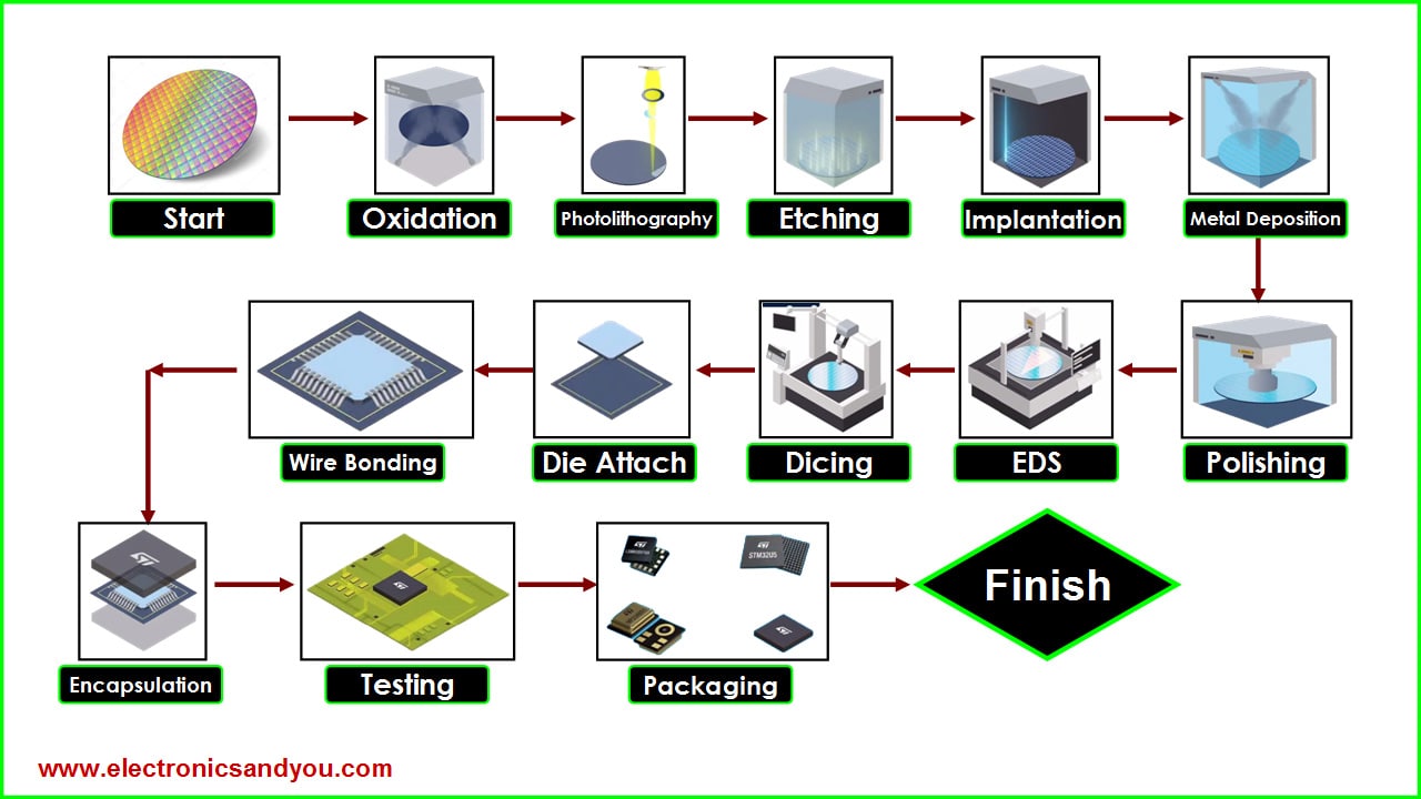 Semiconductor Manufacturing Process Steps Technology Flow
 Semiconductor Engineering Inspecting IC Packages Using Die Sorters
 Securosis Blog Article
 A Process Flow Of Chip to wafer Bonding With Cu SnAg Microbumps Through
 Selective Catalytic Reduction SCR
  Assembly Processes Semiconductor Optoelectronic OPTOCAP
 Assembly Flow For The XP fcBGA Package Download Scientific Diagram
 IC Test Flow For Advanced Semiconductor Packages AnySilicon
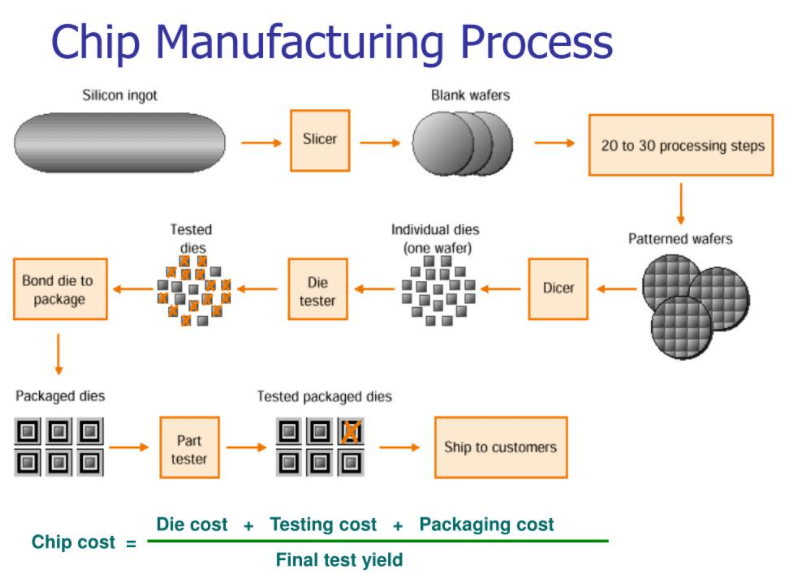 The Electronics Manufacturing Process Electronics R D To Production
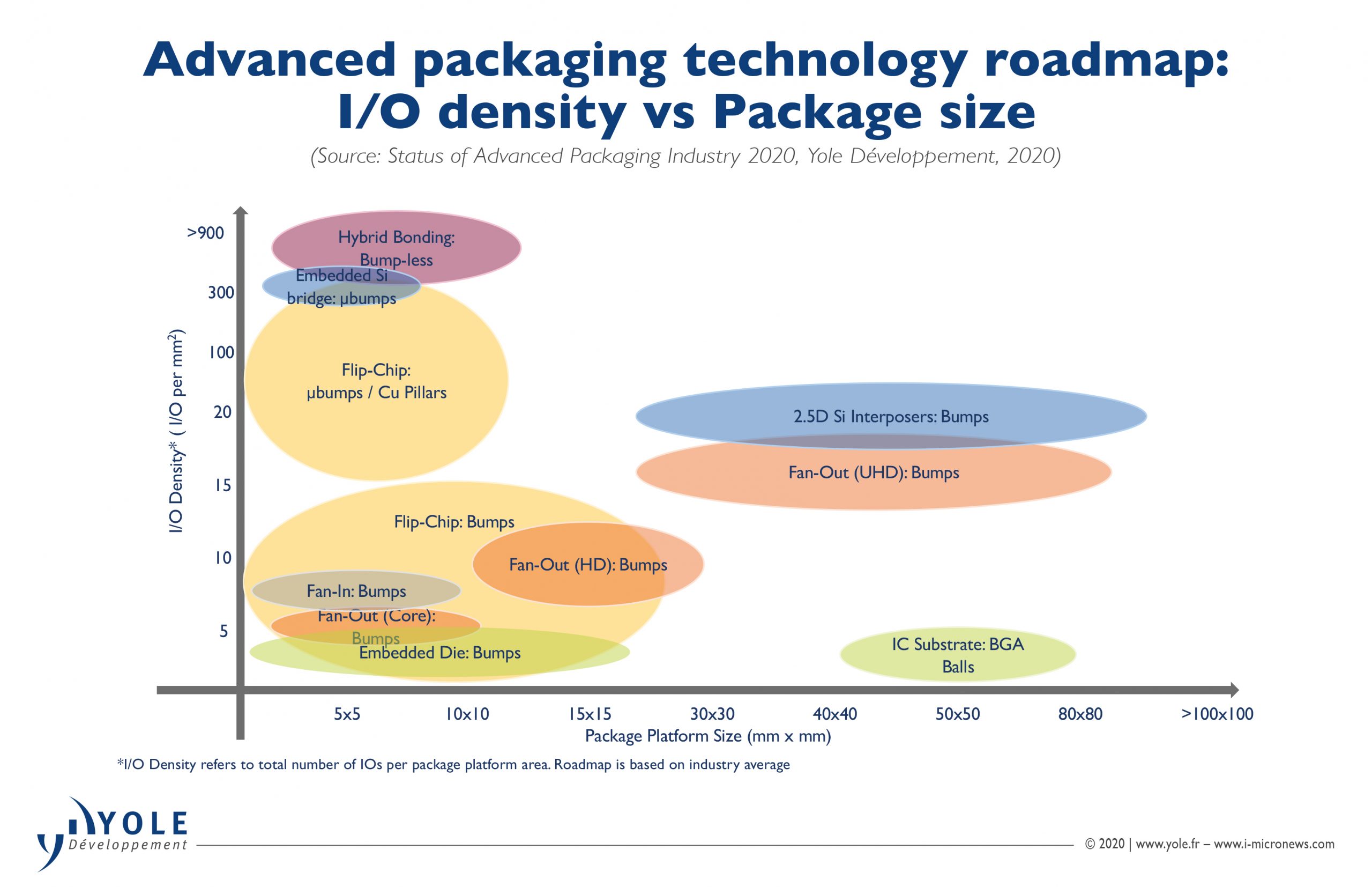 Status Of The Advanced Packaging Industry Semiconductor Digest
 Micromachines Free Full Text A Review Of System in Package
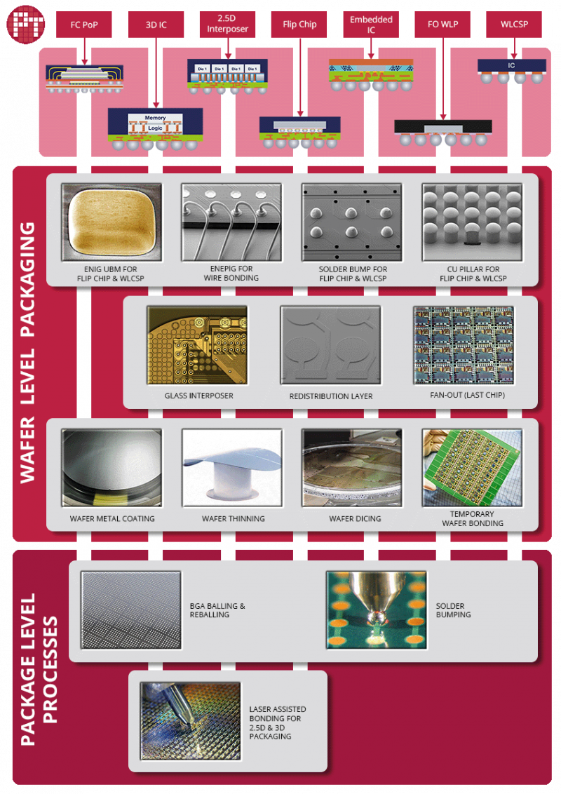 Wafer Level Packaging Services For 3D IC Flip Chip WLCSP